Interconnection structure and forming method thereof
An interconnection structure and interconnection layer technology, applied in electrical components, electrical solid devices, circuits, etc., can solve the problems of occupying the effective area of the circuit, reducing the effective utilization rate of the circuit design area, and reducing the degradation of the gate oxide layer. , the effect of reducing the degradation phenomenon and reducing the area
- Summary
- Abstract
- Description
- Claims
- Application Information
AI Technical Summary
Problems solved by technology
Method used
Image

Examples
Embodiment 1
[0052] Embodiment 1: Reference image 3 and Figure 4 What is shown is a schematic cross-sectional structure diagram of the first embodiment of the method for forming an interconnection structure according to the present invention.
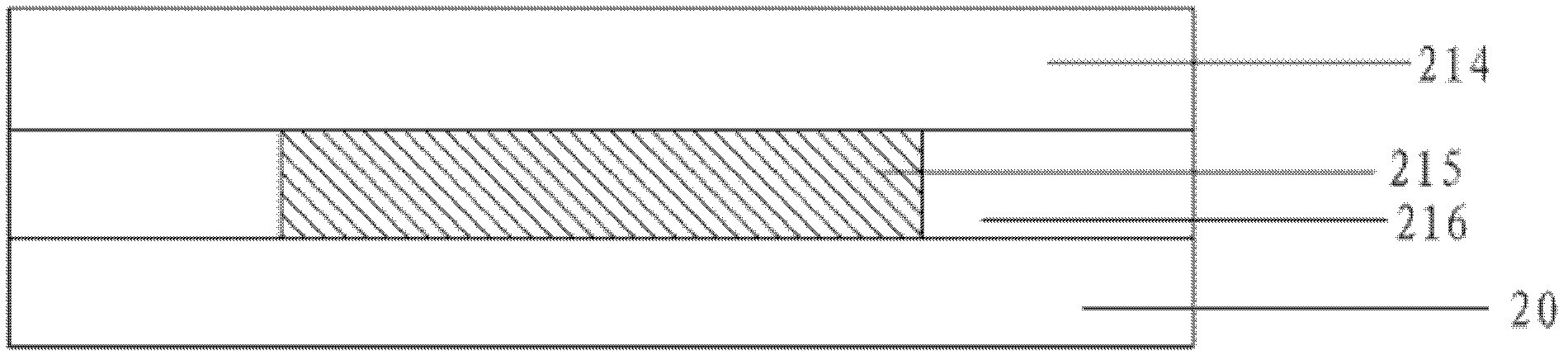
[0053] Specifically, such as image 3 As shown, firstly, a semiconductor substrate 20 is provided, on which there are semiconductor devices. To simplify the diagram, only a blank semiconductor substrate is shown here.
[0054] Then, an interconnection structure is formed on the semiconductor substrate 20 , the interconnection structure includes a metal layer 215 , and the metal layer 215 is located in the insulating dielectric layer 216 and is flush with the surface of the insulating dielectric layer 216 . Optionally, the material of the metal layer 215 is copper, and the material of the insulating dielectric layer 216 is silicon oxide. The specific process for forming the insulating dielectric layer 216 and the metal layer 215 is the prior art...
Embodiment 2
[0063] Embodiment 2: Reference Figure 5 and Figure 6 What is shown is a schematic cross-sectional structure diagram of the second embodiment of the method for forming an interconnection structure according to the present invention.
[0064] Specifically, such as Figure 5 As shown, firstly, a semiconductor substrate 20 is provided, on which there are semiconductor devices. To simplify the diagram, only a blank semiconductor substrate is shown here.
[0065] Then, an interconnection structure is formed on the semiconductor substrate 20 , the interconnection structure includes metal layers 215 , 219 , and the metal layers 215 , 219 are located in the insulating dielectric layer 216 and flush with the surface of the insulating dielectric layer 216 . Optionally, the material of the metal layers 215 and 219 is copper, and the material of the insulating dielectric layer 216 is silicon oxide. The specific process method for forming the insulating dielectric layer 216 and the met...
Embodiment 3
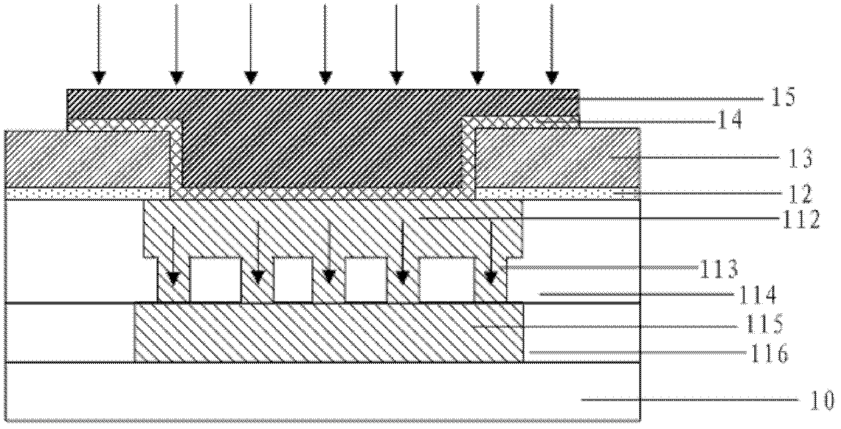
[0072] Embodiment three: reference Figure 7 A schematic diagram of a first embodiment of an interconnection structure of the present invention including pads is shown. This embodiment is a schematic diagram of forming an interconnection structure including pads by performing a back-end process on the basis of the interconnection structure formed in the first embodiment above.
[0073] Specifically, as Figure 7 As shown, first, the first dielectric barrier layer 22 is formed on the interlayer dielectric layer 214 and the metal wiring layer 212, wherein the material of the first dielectric barrier layer 22 is silicon nitride or silicon carbide or silicon carbonitride . The function of the first dielectric barrier layer 22 is to prevent the subsequent passivation layer 23 from oxidizing the metal wiring layer 212 .
[0074] Then, a passivation layer 23 is formed on the first dielectric barrier layer 22, wherein the material of the passivation layer 23 is silicon oxide. Opti...
PUM
 Abstract
Description
Claims
Application Information
 - R&D
- Intellectual Property
- Life Sciences
- Materials
- Tech Scout
- Unparalleled Data Quality
- Higher Quality Content
- 60% Fewer Hallucinations
Browse by: Latest US Patents, China's latest patents, Technical Efficacy Thesaurus, Application Domain, Technology Topic, Popular Technical Reports.
© 2025 PatSnap. All rights reserved.Legal|Privacy policy|Modern Slavery Act Transparency Statement|Sitemap|About US| Contact US: help@patsnap.com