Led package structure and method of fabricating the same
A technology of light-emitting diodes and packaging structures, applied to semiconductor devices, electrical components, circuits, etc., can solve the problems of light-emitting chips 13 such as poor light-emitting efficiency, luminous characteristics, and uneven thickness, and achieve optimal airtightness and high luminous efficiency. Effect
- Summary
- Abstract
- Description
- Claims
- Application Information
AI Technical Summary
Problems solved by technology
Method used
Image

Examples
no. 1 example
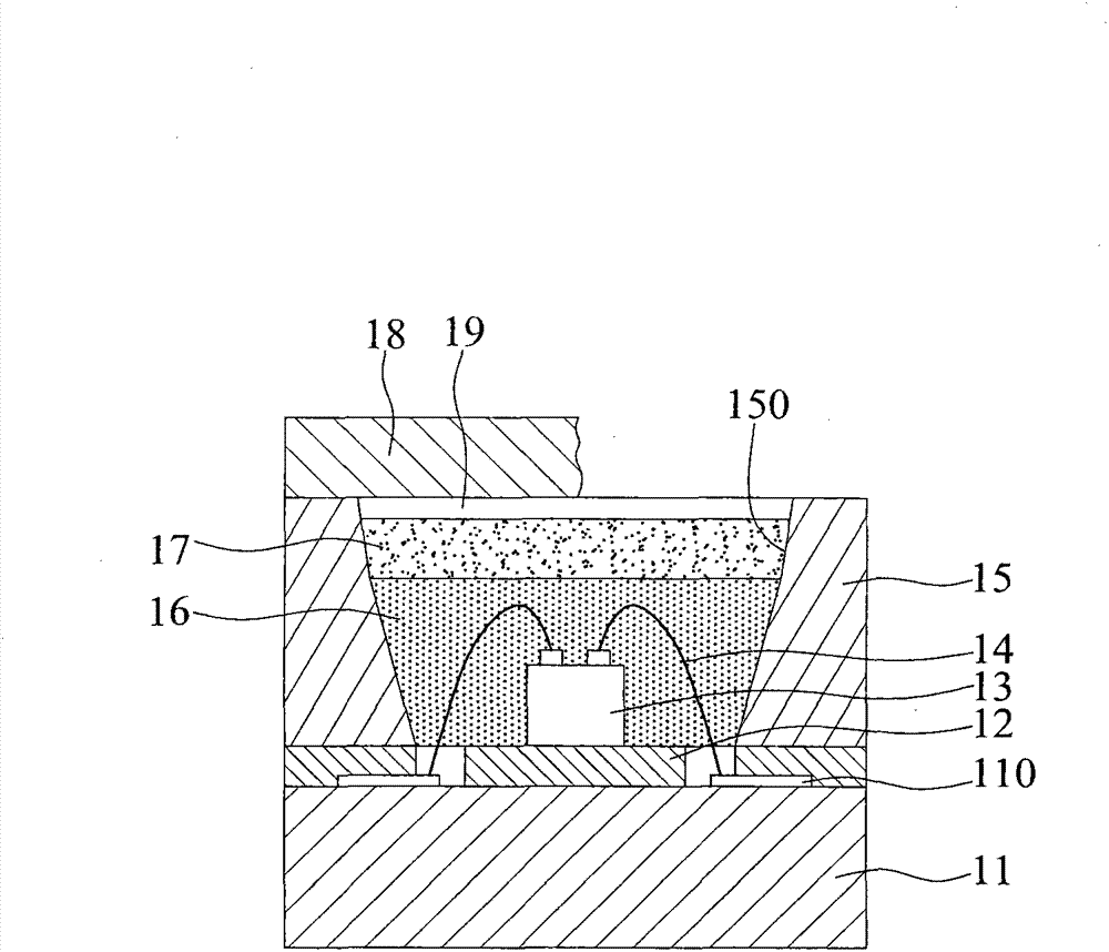
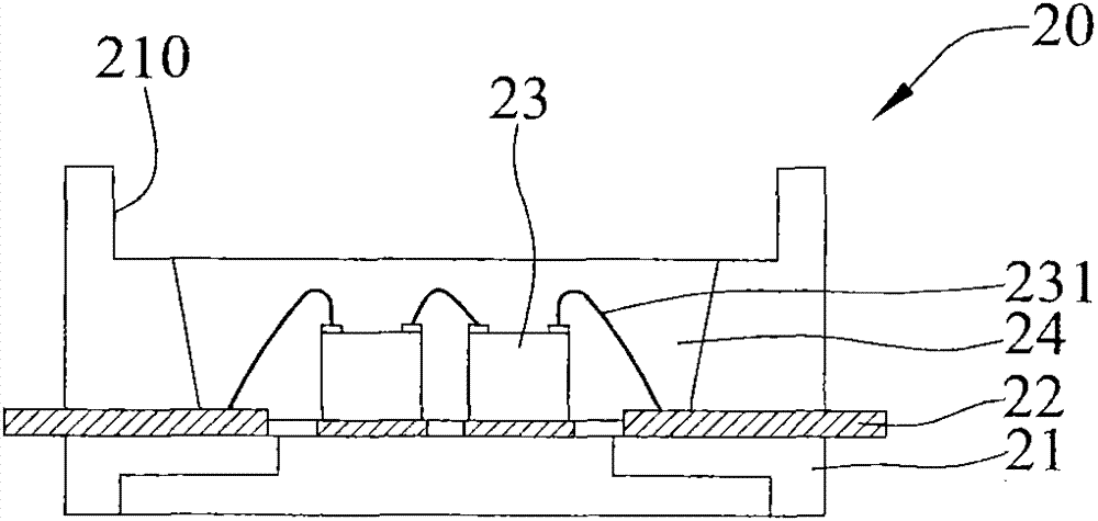
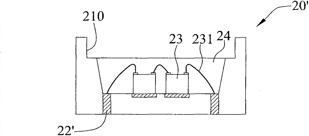
[0024] see Figure 2A to Figure 2E ", which is used to illustrate the manufacturing method of the first embodiment of the light emitting diode packaging structure of the present invention.
[0025] Such as Figure 2A and Figure 2A 'As shown, firstly, a packaging unit 20 is provided, the packaging unit 20 includes a seat body 21 having a groove 210, a guide pin 22 set in the groove 210 and extending to the outside of the seat body 21, and a guide pin 22 set in the groove The light-emitting chip 23 on the bottom surface of the groove 210, the conductive element 231 electrically connecting the light-emitting chip 23 and the lead 22, and the second light-transmitting packaging material 24 filled in the groove 210 and covering the lead 22 , light emitting chip 23 and conductive element 231, such as Figure 2A As shown, the conductive element 231 is a bonding wire. Of course, the light-emitting chip 23 can also be electrically connected to the lead 22 through a bump in a flip-ch...
no. 2 example
[0032] see Figure 3A to Figure 3C , which is used to illustrate the manufacturing method of the second embodiment of the light emitting diode packaging structure of the present invention, the difference from the above is the manufacturing method of the frame structure.
[0033] Such as Figure 3A shown, providing a preceding Figure 2A ’ structure; then, seal the first light-transmitting member 25 in the groove 210, and then set the frame structure 26 on the edge of the groove 210.
[0034] Such as Figure 3B As shown, the first accommodating space 26a is filled with a first light-transmitting packaging material 27, and the volume of the first light-transmitting packaging material 27 is larger than that of the first accommodating space 26a.
[0035] Such as Figure 3C and Figure 3C ’, the second light-transmitting member 28 is combined on the frame structure 26, and the excess first light-transmitting packaging material 27 is squeezed into the second accommodating space...
no. 3 example
[0037] see Figure 4A to Figure 4C ’, which is used to illustrate the manufacturing method of the third embodiment of the light emitting diode packaging structure of the present invention, and the difference from the above lies in the manufacturing method of the frame structure.
[0038] Such as Figure 4A shown, providing the same as previously described Figure 2A 'The structure shown; then, seal the first light-transmitting member 25 in the groove 210, and then set the inner frame 261 on the first light-transmitting member 25, and the outer frame 262 is arranged in the groove 210 , the inner frame 261 has a first accommodating space 26 a , and a second accommodating space 26 b is formed between the inner frame 261 and the outer frame 262 .
[0039] Such as Figure 4B As shown, the first accommodating space 26a is filled with a first light-transmitting packaging material 27, and the volume of the first light-transmitting packaging material 27 is larger than that of the fi...
PUM
 Abstract
Description
Claims
Application Information
 - Generate Ideas
- Intellectual Property
- Life Sciences
- Materials
- Tech Scout
- Unparalleled Data Quality
- Higher Quality Content
- 60% Fewer Hallucinations
Browse by: Latest US Patents, China's latest patents, Technical Efficacy Thesaurus, Application Domain, Technology Topic, Popular Technical Reports.
© 2025 PatSnap. All rights reserved.Legal|Privacy policy|Modern Slavery Act Transparency Statement|Sitemap|About US| Contact US: help@patsnap.com