
Power semiconductor device having plurality of switching elements connected in parallel

A semiconductor and power technology, applied in the field of power semiconductor devices, can solve problems such as inability to apply, turn-off loss without considering turn-on loss, etc., and achieve the effect of reducing switching loss

Active Publication Date: 2012-11-07
MITSUBISHI ELECTRIC CORP
View PDF7 Cites 19 Cited by
  • Summary
  • Abstract
  • Description
  • Claims
  • Application Information

AI Technical Summary

Problems solved by technology

[0007] In the above-mentioned Japanese Patent Application Laid-Open No. 5-291913, although the reduction of the switching loss is considered, only the reduction of the turn-off loss is considered and the turn-on loss is not considered.
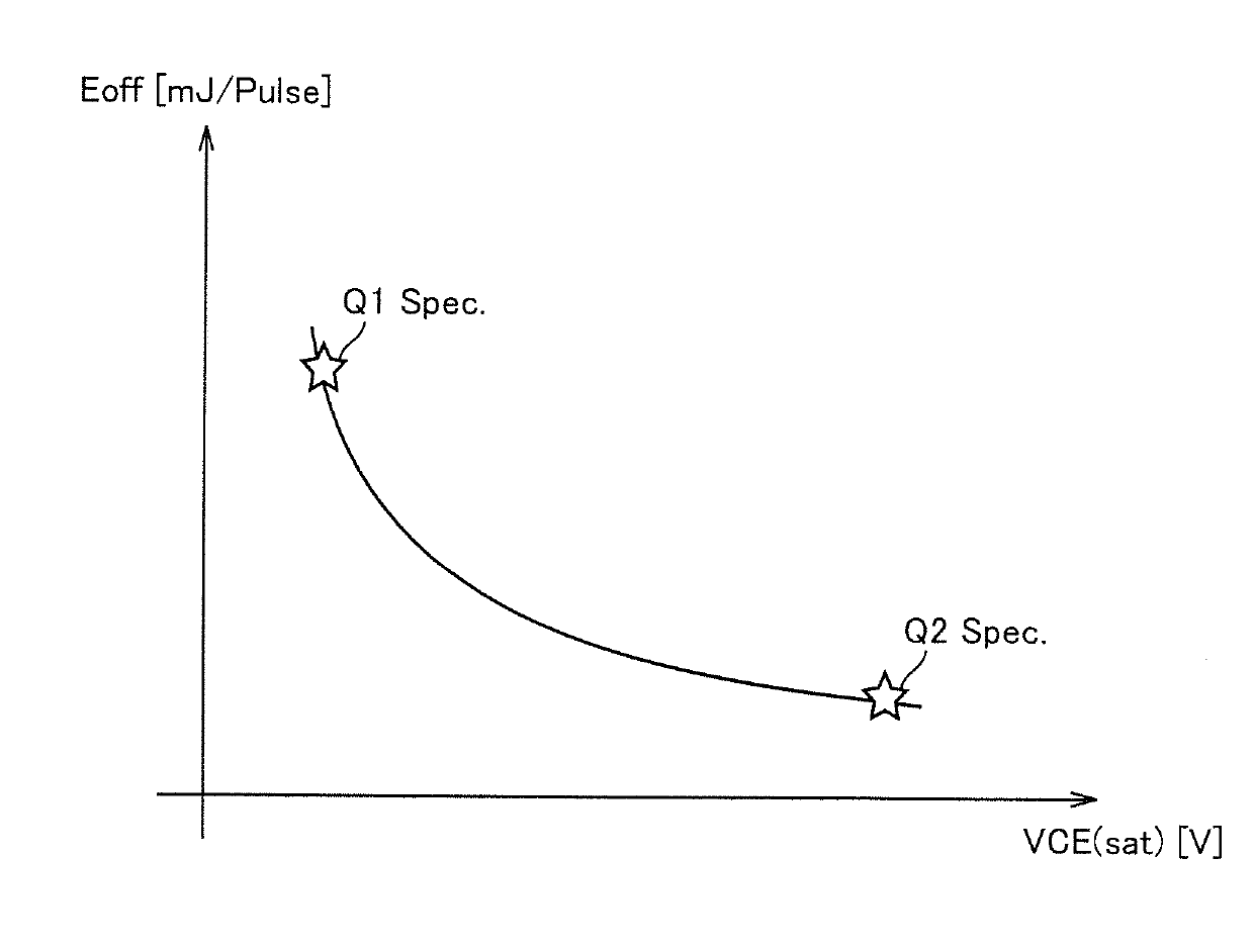
Also, since the method described in this document is a method of parallel-connecting a first IGBT having a low saturation voltage and a long fall time and a second IGBT having a high saturation voltage and a short fall time, in the same characteristic Cannot be used when power semiconductor elements are connected in parallel

Method used


Image

  • Power semiconductor device having plurality of switching elements connected in parallel
  • Power semiconductor device having plurality of switching elements connected in parallel
  • Power semiconductor device having plurality of switching elements connected in parallel

Examples


Embodiment approach 1

[0054] [Structure of Power Semiconductor Device 200 ]

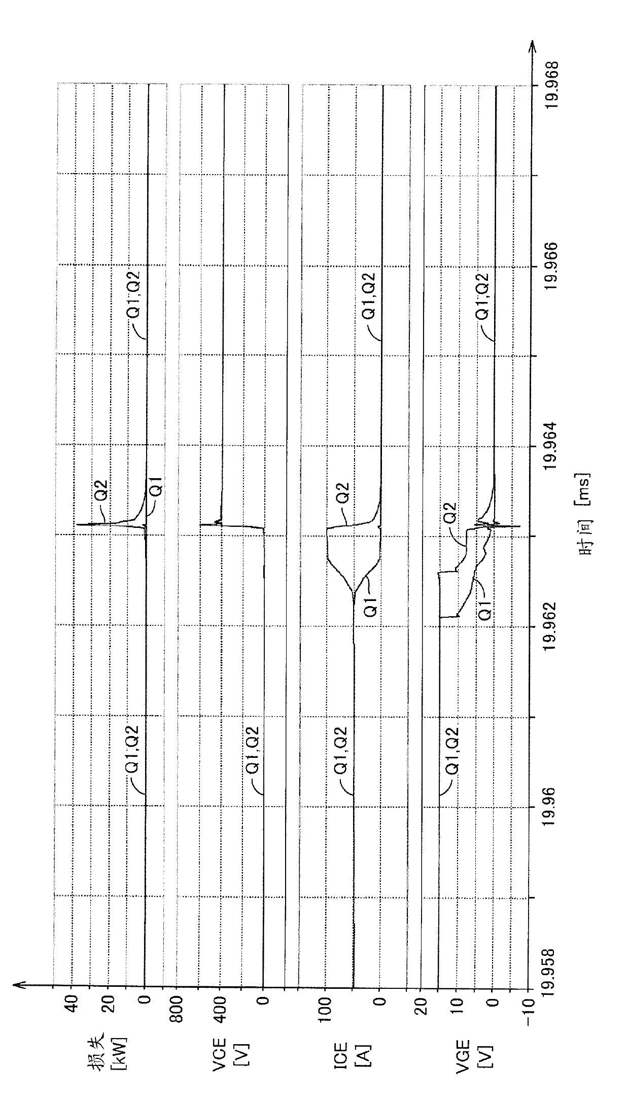
[0055] figure 1 It is a configuration diagram of the power semiconductor device 200 according to Embodiment 1 of the present invention. refer to figure 1 The power semiconductor device 200 includes the power semiconductor elements Q1 and Q2 connected in parallel between the high voltage node HV and the ground node GND, and the drive control unit 100 . exist figure 1 In the above, IGBTs are exemplified as power semiconductor elements Q1 and Q2 , but other semiconductor elements such as power MOSFETs and bipolar transistors may also be used. Hereinafter, the power semiconductor elements Q1 and Q2 are also referred to as IGBT Q1 and Q2, respectively. The high-voltage node HV to which the collectors of IGBT Q1 and Q2 are connected is connected to an electric device to be controlled, and a high voltage is applied thereto.

[0056] Drive control unit 100 switches IGBT Q1 and Q2 into an on state or an off state according to...

Embodiment approach 2

[0115] Figure 17 It is a circuit diagram showing the configuration of the power semiconductor device 201 according to Embodiment 2 of the present invention. Shown in Embodiment 2 figure 1 An example of the specific structure of the drive control unit 100. Figure 17 The drive control unit 101 includes: integrated circuit (IC: Integrated Circuit) 5 for control; power supply V1 for drive; resistance elements R14, R15, R23, R24; N-type MOS (Metal Oxide Semiconductor: metal oxide semiconductor) transistors Q11, Q22, Q33, Q44.

[0116] The integrated circuit 5 includes: an input terminal IN for receiving the driving signal DS; and output terminals OUT1, OUT2, OUT3, and OUT4 for outputting control signals corresponding to the driving signal DS to the gates of the transistors Q11, Q22, Q33, and Q44, respectively. The drains of the transistors Q11 and Q33 are connected to the power supply node 9 to which a driving voltage is supplied from the driving power supply V1. The sources ...

Embodiment approach 3

[0127] Figure 19 It is a circuit diagram showing the configuration of the power semiconductor device 202 according to Embodiment 3 of the present invention. Shown in Embodiment 3 figure 1 An example of the specific structure of the drive control unit 100. Figure 19 The drive control unit 102 includes: integrated circuit (IC) 5a for control; power supply V1 for drive; resistance elements R14, R15, R23, R24; N-type MOS transistors Q11, Q22, Q33, Q44 for driving IGBTQ1, Q2 ; Delay circuits DLY1, DLY2.

[0128] The integrated circuit 5a includes: an input terminal IN for receiving the drive signal DS; for outputting a control signal corresponding to the drive signal DS to the gate of the transistor Q11 and an output terminal OUT1 of the delay circuit DLY1; for outputting a control signal corresponding to the drive signal DS The control signal is output to the gate of the transistor Q22 and the output terminal OUT2 of the delay circuit DLY2. The drains of the transistors Q11 ...


PUM


Abstract

The invention relates to a power semiconductor device having a plurality of switching elements connected in parallel. The power semiconductor device (200) possesses a first power semiconductor element (Q1), a second power semiconductor element (Q2) and a driving control part (100). The driving control part (100) enables the first and second power semiconductor elements to switch to a conductive or stop state according to the conduction or stop instruction reveived from the exterior. Specifically, the condition that the first and second power semiconductor elements (Q1, Q2) switch to the conduction state simultaneously and the condition that the one of the first and second power semiconductor elements (Q1, Q2) switches to the conduction state and then the other switches to the conduction state can be switched through the driving control part (100). The driving control part (100) enables one of the first and second power semiconductor elements (Q1, Q2) to switch to the stop state and then the other switch to the stop state according to the stop instruction.

Description

technical field [0001] The present invention relates to a power semiconductor device used in power conversion equipment and the like. Background technique [0002] Power semiconductor devices such as power MOSFETs (Metal-Oxide-Semiconductor Field-Effect Transistor: Metal-Oxide-Semiconductor Field-Effect Transistor) or IGBT (Insulated Gate Bipolar Transistor: Insulated Gate Bipolar Transistor) are used in motor drive inverters ( Inverter), uninterruptible power supply device and frequency conversion device and other power equipment control. Since the rated voltage and rated current of these power devices tend to increase, higher withstand voltage and higher current are also required for power semiconductor elements. [0003] As a method of increasing the amount of current controlled by a power semiconductor element, a method of connecting a plurality of power semiconductor elements in parallel is known (for example, refer to Japanese Patent Application Laid-Open No. 2000-928...

Claims


Application Information

Patent Timeline
Patent Type & Authority Applications(China)
IPC IPC(8): H02M1/08
CPCH03K2217/0036H03K17/164H03K17/168H03K17/127H02M1/08H03K17/12
Inventor 候賽因·哈利德·哈桑熊谷敏之齐藤省二
Owner MITSUBISHI ELECTRIC CORP
Learn More