Electronic component moving test device and method
A technology of electronic components and mobile testing, which is applied in the direction of measuring devices, measuring device casings, measuring electronics, etc., can solve the problems of low production efficiency, time-consuming and laborious, etc., and achieve the effect of improving production efficiency and reducing costs
- Summary
- Abstract
- Description
- Claims
- Application Information
AI Technical Summary
Problems solved by technology
Method used
Image
Examples
Embodiment 1
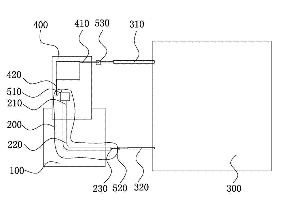
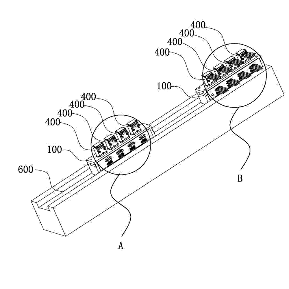
[0061] A mobile testing device for electronic components, including a carrying fixture 100 and a testing instrument 300 .
[0062] The carrying fixture 100 includes a conductor 200, and the conductor 200 includes an element connection end 210 for connecting the electronic element 400, an instrument connection end 230 for connecting the testing instrument 300, and an instrument connection end 230 for connecting the element connection end 210 and the instrument connection end 230. The connection part 220;
[0063] The detection instrument 300 is provided with a component contact part 310 for contacting the electronic component 400 and an instrument contact part 320 for contacting the instrument connection end 230;
[0064] The electronic component 400, the conductor 200 and the testing instrument 300 are sequentially connected to form a test circuit.
[0065] The carrying jig 100 is integrally formed as a carrying jig. The carrying jig 100 has good integrity and can firmly cla...
Embodiment 2
[0072] The main technical solutions of this embodiment are the same as those of Embodiment 1, and the features not explained in this embodiment are explained in Embodiment 1, and will not be repeated here. The difference between this embodiment and embodiment 1 is:
[0073] Such as figure 2 As shown, the component connection end 210 is fixedly connected to the connection plug 211 .
[0074] The carrying jig 100 includes a base 140 , a first splint 120 , a second splint 130 and an upper cover 110 . The base 140 defines a slot 141 through which the wire 231 of the component connecting end 210 passes. Both the component connection end 210 and the instrument connection end 230 are exposed outside the carrying fixture 100 , the component connection end 210 is connected to the electronic component 400 , and the instrument connection end 230 is connected to the testing instrument 300 .
[0075] The first clamping plate 120 and the second clamping plate 130 for clamping the compon...
Embodiment 3
[0080] The main technical solutions of this embodiment are the same as those of Embodiment 2, and the features not explained in this embodiment are explained in Embodiment 2, and will not be repeated here. The difference between this embodiment and embodiment 2 is:
[0081] Such as image 3 , Figure 4 , Figure 5 and Figure 6 As shown, the instrument connection end 230 is connected to a circuit board 232 through a wire 231 , and the circuit board 232 is welded with an output terminal 233 . The wire 231 is welded to the welding point 2321 of the circuit board 232 , and the circuit board 232 is fixed to the carrying fixture 100 .
[0082] Specifically, the output terminal 233 is a metal probe. The metal probe is welded to the terminal hole 2322 of the circuit board 232 , and is electrically connected to the wire 231 through the soldering point 2321 by the wiring on the circuit board 232 . The setting of the output terminal 233 makes the connection between the instrument ...
PUM
 Abstract
Description
Claims
Application Information
 - R&D
- Intellectual Property
- Life Sciences
- Materials
- Tech Scout
- Unparalleled Data Quality
- Higher Quality Content
- 60% Fewer Hallucinations
Browse by: Latest US Patents, China's latest patents, Technical Efficacy Thesaurus, Application Domain, Technology Topic, Popular Technical Reports.
© 2025 PatSnap. All rights reserved.Legal|Privacy policy|Modern Slavery Act Transparency Statement|Sitemap|About US| Contact US: help@patsnap.com


