One-way perspective glass and preparation method thereof
A one-way perspective glass and glass substrate technology, which is applied in the field of electric light sources, can solve the problems that one-way perspective glass cannot achieve one-way perspective, the one-way perspective glass has a reduced perspective, and artificial traces are too obvious, so as to ensure the visibility. , Reduce observation interference and achieve the effect of perspective effect
- Summary
- Abstract
- Description
- Claims
- Application Information
AI Technical Summary
Problems solved by technology
Method used
Image
Examples
preparation example Construction
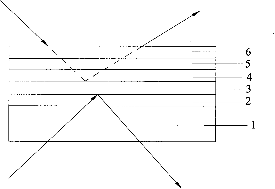
[0034] The embodiment of the present invention also provides the preparation method of the above-mentioned one-way see-through glass, the process flow chart of the method is as follows image 3 shown, see also figure 1 or figure 2 or image 3 , the method includes the following steps:
[0035] S1. Provide glass substrate 1;
[0036] S2. Plating a composite dielectric layer 2 on one surface of the glass substrate 1;
[0037] S3. Plating a metal reflective layer 3 on the composite dielectric layer 2;
[0038] S4. Plating a stop metal oxide layer 4 on the metal reflective layer 3;
[0039] S5. Plating a light absorbing layer 5 on the metal oxide layer 4;
[0040] S6. Plating a composite dielectric protective layer 6 on the light absorbing layer 5 .
[0041] Specifically, the step S1 of the above-mentioned one-way glass preparation method preferably includes pre-treatment of the glass substrate 1 . The pre-treatment may include cleaning with chemical reagents, ultrasonic ...
Embodiment 1
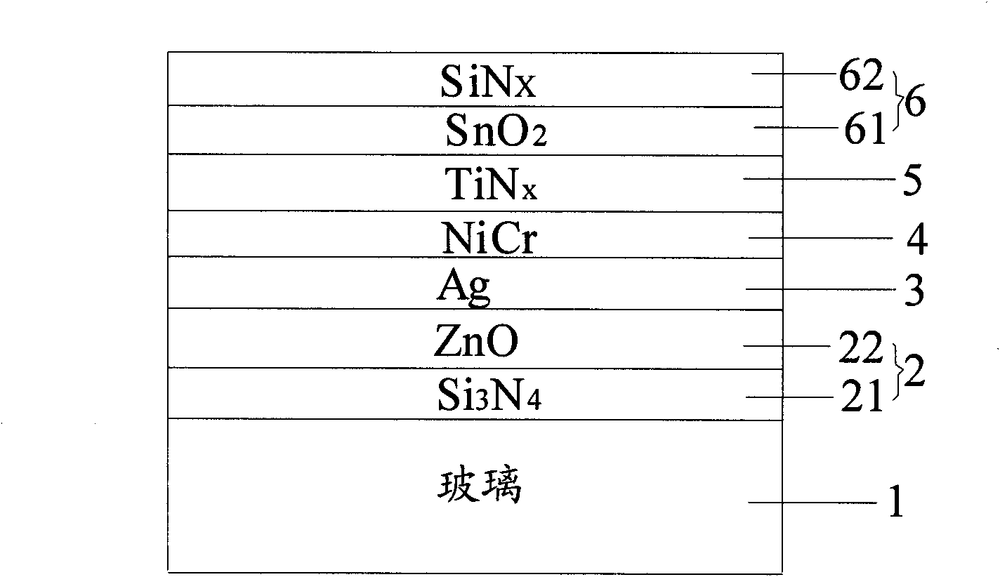
[0052] The one-way see-through glass structure of this embodiment is as figure 2 As shown, the one-way see-through glass includes ordinary white glass substrates 1, Si 3 N 4 Layer 21, ZnO layer 22, Ag layer 3, NiCr layer 4, TiN x Layer 5, SnO 2 layer 61 and SiN x Layer 62. Among them, Si 3 N 4 The thickness of layer 21 is 22nm, the thickness of ZnO layer 22 is 12nm, Si 3 N 4 Layer 21 and ZnO layer 22 constitute composite dielectric layer 2; Ag layer 3 has a thickness of 26nm; NiCr layer 4 has a thickness of 3nm; TiN x The thickness of layer 5 is 26nm; SnO 2 Layer 61 has a thickness of 20nm, SiN x Layer 62 has a thickness of 20nm, SnO 2 layer 61 and SiN x Layer 62 constitutes the composite dielectric protection layer 6 .
[0053] Its preparation method is: utilize flat glass double-end continuous coating machine, adopt the technological parameter listed in the following table 1, use 6 alternating current rotating cathodes, 2 direct current planar cathodes, altoget...
Embodiment 2
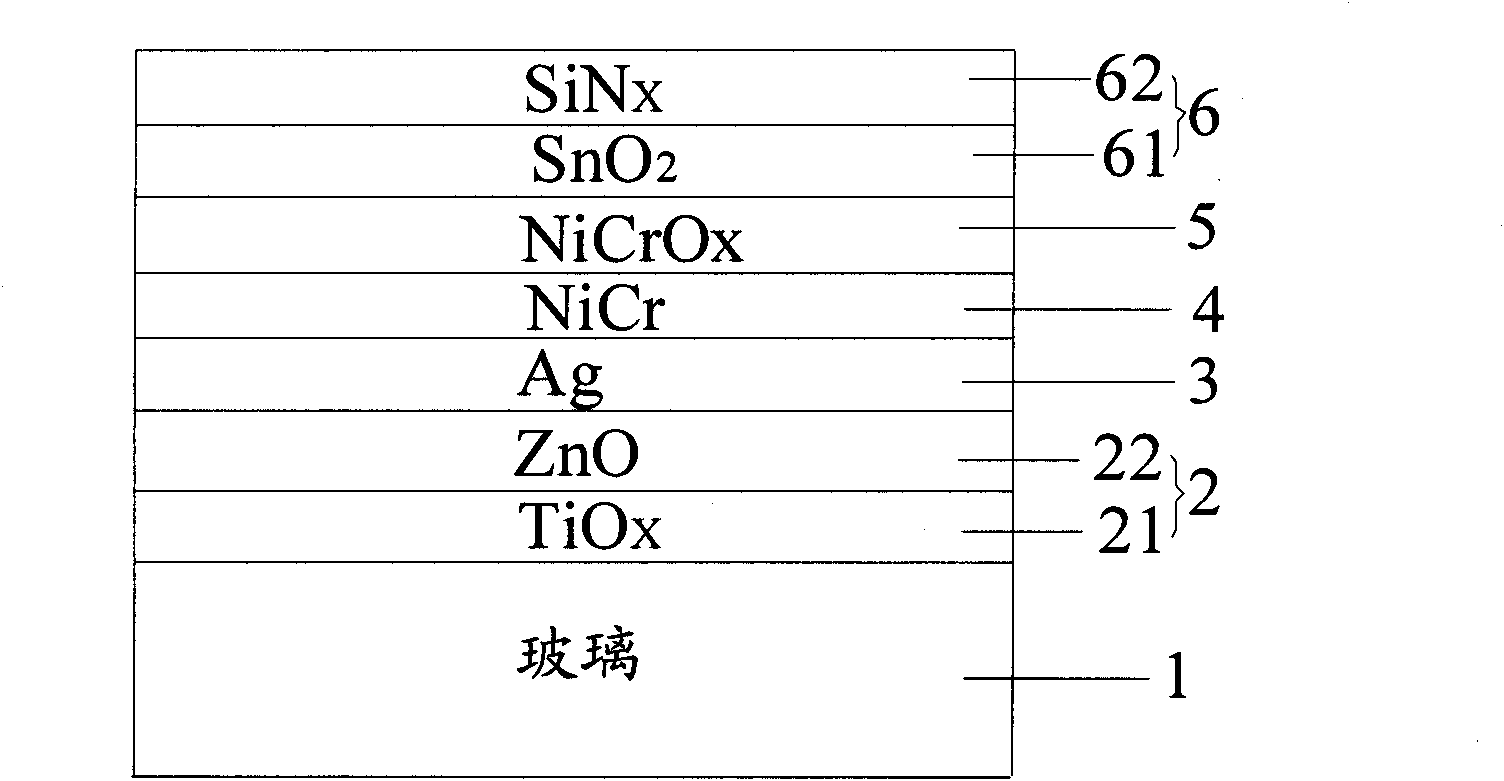
[0061] The one-way see-through glass structure of this embodiment is as image 3 As shown, the one-way see-through glass includes ordinary white glass substrate 1, TiO x Layer 21, ZnO layer 22, Ag layer 3, NiCr layer 4, NiCrO x Layer 5, SnO 2 layer 61 and SiN x Layer 62. Among them, TiO x The thickness of layer 21 is 14nm, the thickness of ZnO layer 22 is 10nm, TiO x Layer 21 and ZnO layer 22 constitute composite dielectric layer 2; Ag layer 3 has a thickness of 26nm; NiCr layer 4 has a thickness of 2nm; NiCrO x The thickness of layer 5 is 27nm; SnO 2 Layer 61 has a thickness of 17nm, SiN xLayer 62 has a thickness of 20nm, SnO 2 layer 61 and SiN x Layer 62 constitutes the composite dielectric protection layer 6 .
[0062] Its preparation method is: utilize flat glass double-end continuous coating machine, adopt the process parameter listed in the following table 2, use 4 AC rotating cathodes, 3 DC flat cathodes, totally 7 cathodes are produced, and the present invent...
PUM
| Property | Measurement | Unit |
|---|---|---|
| thickness | aaaaa | aaaaa |
| thickness | aaaaa | aaaaa |
| thickness | aaaaa | aaaaa |
Abstract
Description
Claims
Application Information
 - R&D
- Intellectual Property
- Life Sciences
- Materials
- Tech Scout
- Unparalleled Data Quality
- Higher Quality Content
- 60% Fewer Hallucinations
Browse by: Latest US Patents, China's latest patents, Technical Efficacy Thesaurus, Application Domain, Technology Topic, Popular Technical Reports.
© 2025 PatSnap. All rights reserved.Legal|Privacy policy|Modern Slavery Act Transparency Statement|Sitemap|About US| Contact US: help@patsnap.com


