Multilayer electromagnetic wave absorbing structure
A technology of wave structure and electromagnetic wave, applied in the field of electromagnetic wave absorbing structure and its design, to achieve the effect of strong operability, good wave absorbing performance and simple process
- Summary
- Abstract
- Description
- Claims
- Application Information
AI Technical Summary
Problems solved by technology
Method used
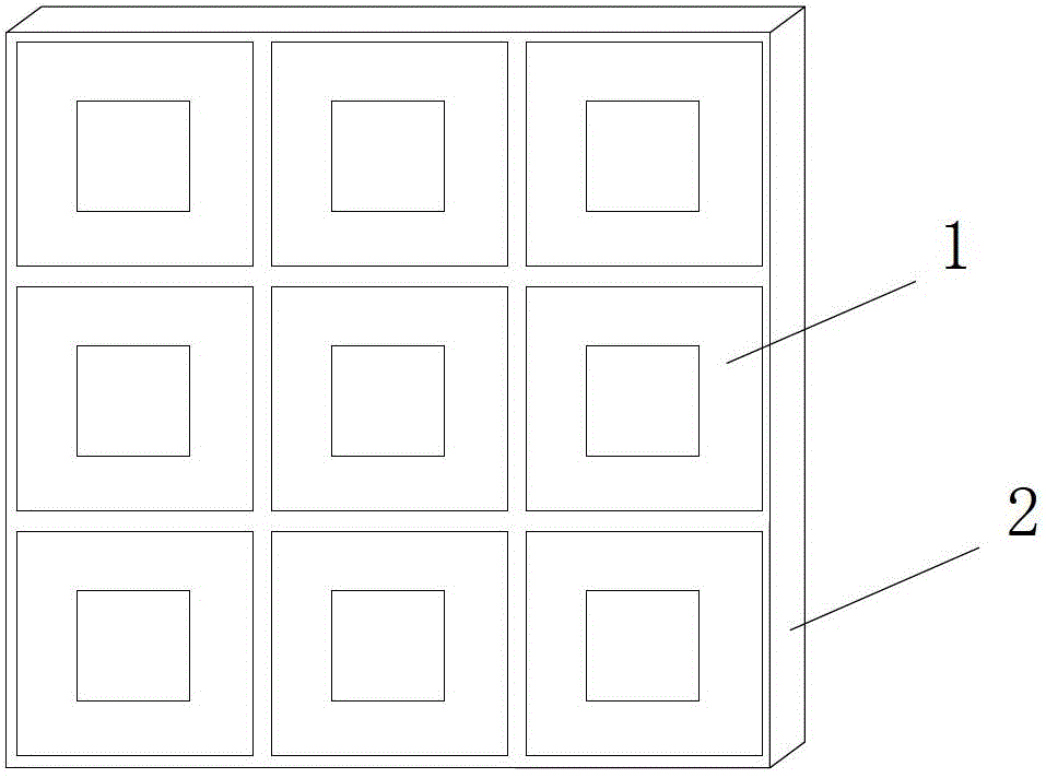
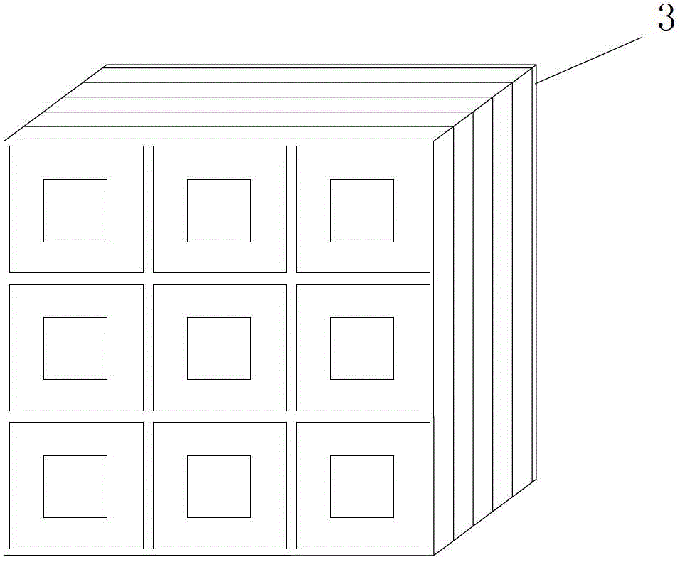
Image

Examples
Embodiment 1
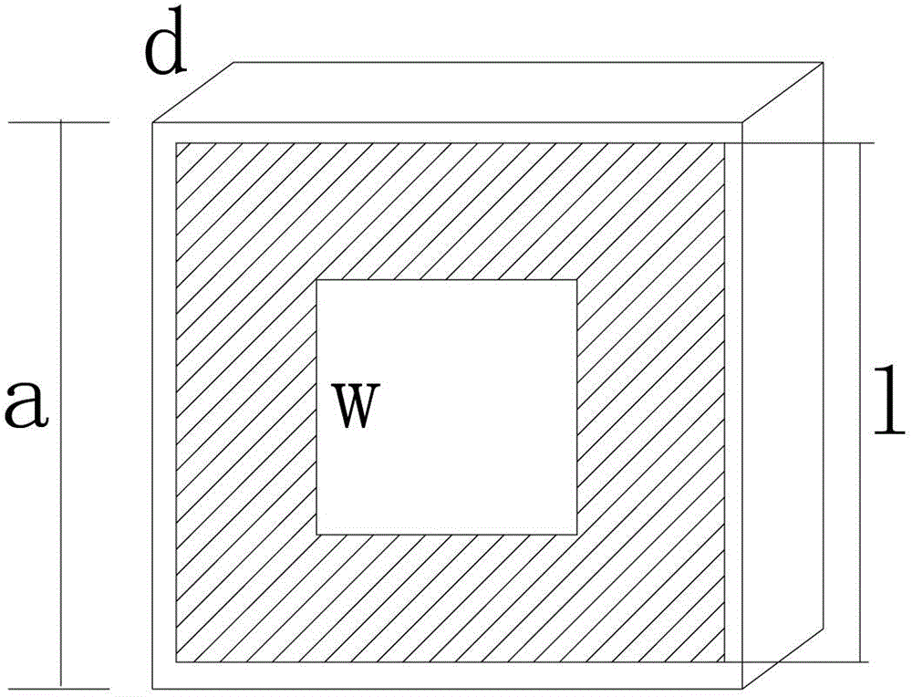
[0020] A 4-layer light-weight broadband square pattern absorbing structure, its specific size parameters are (in mm): a 1 =15.7, l 1 =15, w 1 =5.2, d 1 =5, r 1 =50Ω / □; a 2 =15.7,l 2 =11.1,w 2 =8.1, d 2 =5, r 2 =70Ω / □; a 3 =15.7, l 3 =15, w 3 =13.6, d 3 =5, r 3 =50Ω / □; a 4 =14.3, l 4 =15, w 4 =12.6, d 4 =5, r 4 =70Ω / □.
[0021] In the case of vertically incident TE or TM waves, this embodiment has Figure 4 The absorbing performance shown. The entire frequency band of 2-18GHz has a reflection coefficient below -10dB, the frequency band of 2.3-18GHz has a reflection coefficient of below -13dB, and the frequency band of 2.5-15GHz has a reflection coefficient of approximately -15dB or less.
Embodiment 2
[0023] A two-layer light-weight broadband square pattern absorbing structure, its specific size parameters are (in mm): a 1 =17,l 1 =16.5,w 1 =8.5, d 1 =5, r 1 =75Ω / □; a 2 =17,l 2 =16.5,w 2 =6.5, d 2 =5, r 2 =110Ω / □.
[0024] In the case of vertically incident TE or TM waves, this embodiment has a reflection coefficient below -7.5dB in the entire frequency band of 2-18GHz, and the frequency bands of 2.3-9.6GHz and 11-17.6GHz have reflection coefficients below -10dB.
Embodiment 3
[0026] A 6-layer light-weight broadband square pattern absorbing structure, its specific size parameters are (in mm): a 1 =12.3, l 1 =11.3, w 1 =6.8, d 1 =5, r 1 =71Ω / □; a 2 =12.3,l 2 =12.3, w 2 =6.6, d 2 =5, r 2 =230Ω / □; a 3 =12.3, l 3 =11.3, w 3 =7.6, d 3 =5, r 3 =230Ω / □; a 4 =12.3, l 4 =10, w 4 =7,d 4 =5, r 4 =230Ω / □; a 5 =12.3,l 5 =10,w 5 =6.1, d 5 =5, r 5 =600Ω / □; a 6 =12.3, l 6 =10,w 6 =7.3, d 6 =5, r 6 =800Ω / □.
[0027] In the case of vertically incident TE or TM waves, this embodiment has a reflection coefficient below -20dB in the entire frequency band of 2-18GHz.
PUM
 Abstract
Description
Claims
Application Information
 - Generate Ideas
- Intellectual Property
- Life Sciences
- Materials
- Tech Scout
- Unparalleled Data Quality
- Higher Quality Content
- 60% Fewer Hallucinations
Browse by: Latest US Patents, China's latest patents, Technical Efficacy Thesaurus, Application Domain, Technology Topic, Popular Technical Reports.
© 2025 PatSnap. All rights reserved.Legal|Privacy policy|Modern Slavery Act Transparency Statement|Sitemap|About US| Contact US: help@patsnap.com