


Quick Research
Generate reliable direction feasibility study reports for your R&D in just a few steps.

Technical Q&A
Discover and master advanced knowledge NOW. Basics, ideas, possibilities, all at once.

Find Solutions
As an expert in R&D theories, this can generate solutions to your technical problems instantly.

Evaluate Feasibility
Analyze your overall solution with one click, know your potential R&D risks in advance.

Monitor Landscape
Get weekly tech updates, stay abreast of the latest tech innovations and key insights.
Tapered-waveguide-assisted cascade long-period waveguide grating sensor and preparation method thereof
A technology of long-period gratings and waveguide gratings, which is applied to optical waveguides, light guides, and optical devices to transmit sensing components and light guides. The effect of response speed
- Summary
- Abstract
- Description
- Claims
- Application Information
AI Technical Summary
Problems solved by technology
Method used
Image

Examples
Embodiment 1
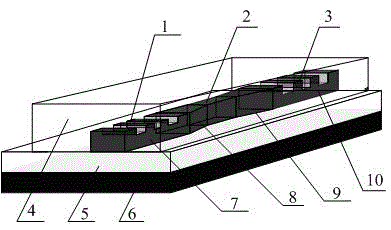
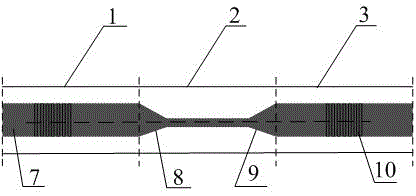
[0024] The cascaded long-period waveguide grating sensor assisted by tapered waveguide is a cascaded long-period grating based on tapered waveguide, see figure 1 Stereogram and figure 2 Top view, composed of three parts: the first long-period waveguide grating (1) is connected to the second long-period waveguide grating (3) through a tapered waveguide (2), and the core refractive index of the three parts is the same, and their The cladding refractive index is also the same.
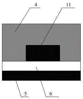
[0025] For the first long-period waveguide grating (1) and the second long-period waveguide grating (3) of the above-mentioned cascaded long-period waveguide gratings assisted by tapered waveguides, see image 3 front view and Figure 4 Side view, etched from polymer waveguide with tapered waveguide, consisting of upper cladding (4), lower cladding (5), substrate (6), core (7) and.
Embodiment 2
[0027] The preparation method of the above-mentioned sensor is as follows: the above-mentioned cascaded long-period waveguide grating based on the tapered waveguide is etched from a polymer waveguide with a tapered waveguide, and first made on silicon-based silicon dioxide by ultraviolet lithography technology. The substrate transfers the tapered waveguide-assisted cascaded waveguide pattern to the photoresist, and then uses the reactive ion etching method to etch the tapered waveguide-assisted cascaded waveguide into a tapered waveguide-assisted cascaded long-period waveguide raster. Its specific process and process steps are as follows:
[0028] 1) Using plasma chemical vapor deposition to deposit a layer of silicon dioxide on the substrate silicon wafer as the lower cladding layer of the optical waveguide, thereby forming a silicon-based silicon dioxide substrate;
[0029] 2) Coat the photoresist uniformly on the surface of silicon-based silicon dioxide by spin coating met...
PUM
 Abstract
Description
Claims
Application Information
 - R&D Engineer
- R&D Manager
- IP Professional
- Industry Leading Data Capabilities
- Powerful AI technology
- Patent DNA Extraction
Browse by: Latest US Patents, China's latest patents, Technical Efficacy Thesaurus, Application Domain, Technology Topic, Popular Technical Reports.
© 2024 PatSnap. All rights reserved.Legal|Privacy policy|Modern Slavery Act Transparency Statement|Sitemap|About US| Contact US: help@patsnap.com