
LED (light-emitting diode) packaging structure using transparent oxide substrate and packaging method thereof

A technology of transparent oxide and junction structure, applied in the direction of electrical components, circuits, semiconductor devices, etc., can solve the problems of poor heat dissipation, limited light output efficiency, unfavorable promotion and application, etc., to improve reliability and consistency, and improve heat dissipation Ability, the effect of improving light extraction efficiency

Inactive Publication Date: 2012-10-03
SUZHOU JINGPIN OPTOELECTRONICS
View PDF4 Cites 9 Cited by
  • Summary
  • Abstract
  • Description
  • Claims
  • Application Information

AI Technical Summary

Problems solved by technology

In order to overcome the above shortcomings, a flip-chip LED chip is proposed, which is to solder the LED chip on the silicon substrate through flip-chip to improve the light output rate; The cost and difficulty of light distribution are not conducive to market promotion and application
[0004] In short, due to a series of problems such as opaque substrates and metal electrode layers, LED chips still can only emit light from one side, which limits the improvement of light emission efficiency and poor heat dissipation; at the same time, the traditional single-chip packaging has a low degree of automation and is not suitable for mass production. Production

Method used


Image

  • LED (light-emitting diode) packaging structure using transparent oxide substrate and packaging method thereof
  • LED (light-emitting diode) packaging structure using transparent oxide substrate and packaging method thereof
  • LED (light-emitting diode) packaging structure using transparent oxide substrate and packaging method thereof

Examples


Embodiment Construction

[0025] The present invention will be further described below in conjunction with the accompanying drawings.

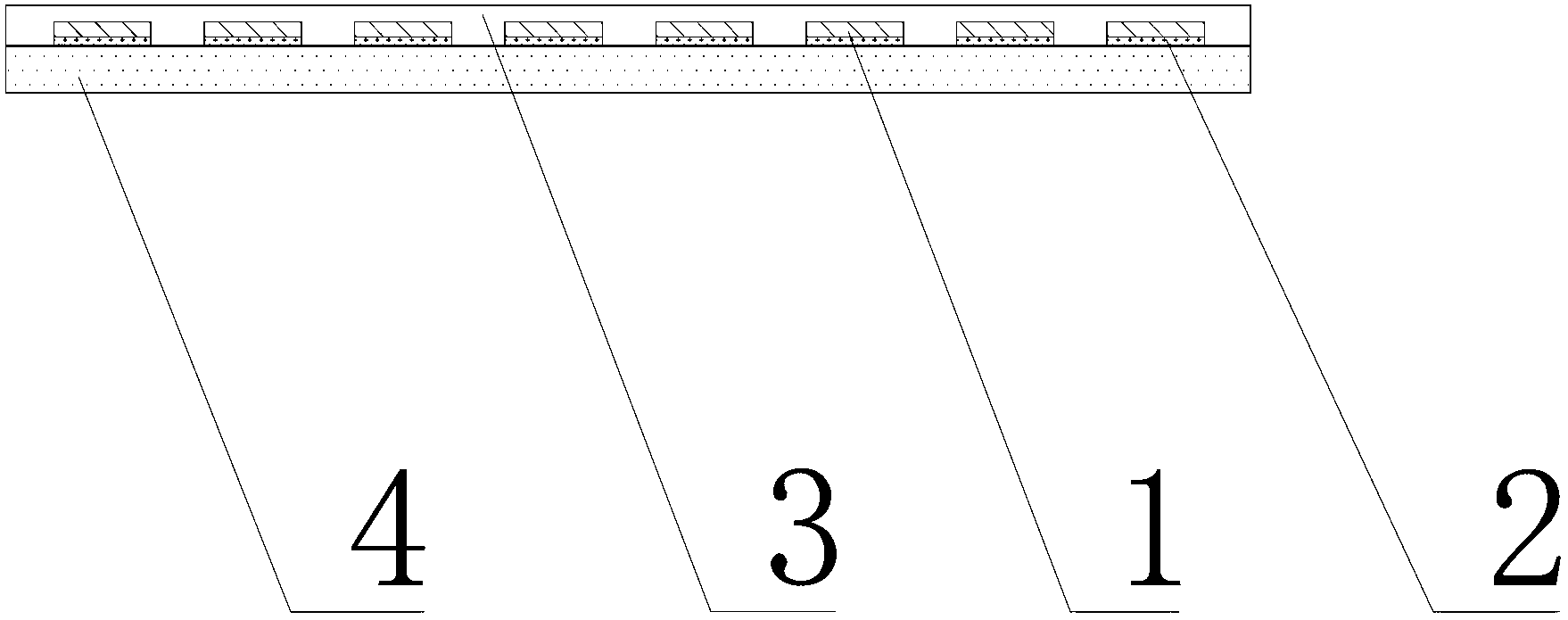
[0026] like figure 1 Shown is an LED sealing structure using a transparent oxide substrate, including a planar transparent oxide substrate 4, a fluorescent film 3 and more than one LED chip 1, and a conductive pattern 2 is arranged on the front of the transparent oxide substrate 4 , an LED bonding area is reserved on the conductive pattern 2, the LED chip 1 is arranged on the LED bonding area, the fluorescent film 3 is plastic-sealed on the front of the transparent oxide substrate 4, and the LED chip is sealed on the transparent oxide substrate 4 and the fluorescent film. Between films 3.

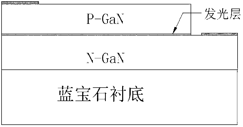
[0027] The LED chip 1 is as figure 2 Mount LED chips as shown or as image 3 The flip-chip LED chip shown; when the LED chip 1 is a front-mounted LED chip, it is connected to the conductive group 2 by jumper wiring.

[0028] The transparent oxide substrate 4 is made of yttrium ...


PUM


Abstract

The invention discloses an LED (Light-Emitting Diode) packaging structure using a transparent oxide substrate, comprising a plane type transparent oxide substrate, a fluorescent thin film and more than one LED chip, wherein a conductive pattern is arranged on the front face of the transparent oxide substrate; an LED bonding region is reserved on the conductive pattern and the LED chips are arrayed on the LED bonding region; and the fluorescent thin film is packaged on the front face of the transparent oxide substrate to seal the LED chips between the transparent oxide substrate and the fluorescent thin film. According to the LED packaging structure using the transparent oxide substrate provided by the invention, a traditional structure for emitting light from one side is broken through, the light emitting efficiency is extremely improved, and the heat radiation capability is improved; the reliability and the consistency of a product are improved by a full-page packaging method, so that the LED packaging structure is suitable for industrial rapid and efficient production; and furthermore, isolating glue is avoided being used and the service life of the product can be prolonged effectively.

Description

technical field [0001] The invention relates to LED packaging technology, in particular to an LED sealing structure using a transparent oxide substrate and a sealing method thereof. Background technique [0002] With the continuous development of LED in the field of lighting, people have higher and higher requirements for its light extraction efficiency. LED packaging materials, packaging structures and packaging methods are all important factors affecting its light extraction efficiency; at present, it is mainly through transparent substrate technology. , metal film reflection technology, flip chip technology to improve the light efficiency of LED. [0003] Usually, blue light and green light LED chips grow GaN (gallium nitride)-based LED chip structure layers on sapphire substrates through MOCVD (metal organic compound chemical vapor deposition) technology, and the light emitted by the P / N junction light-emitting area passes through The upper P-type region is ejected; due...

Claims


Application Information

Patent Timeline
Patent Type & Authority Applications(China)
IPC IPC(8): H01L33/62H01L33/50H01L33/54H01L33/00
Inventor 王媛高鞠
Owner SUZHOU JINGPIN OPTOELECTRONICS
Learn More