Wireless packaging structure of high-power ceramic LED (Light-emitting Diode)

A packaging structure, high-power technology, applied in the direction of electrical components, electrical solid-state devices, circuits, etc., can solve the problems of increasing process costs and material costs, reducing the light-emitting efficiency of light-emitting chips, etc., to reduce complexity, save costs, and improve light output rate effect

Inactive Publication Date: 2012-10-03
ZHEJIANG INTELED OPTOELECTRONICS TECH
View PDF5 Cites 5 Cited by
  • Summary
  • Abstract
  • Description
  • Claims
  • Application Information

AI Technical Summary

Problems solved by technology

[0004] The invention mainly solves the problem that the LED lamp adopts the wire bonding process in the prior art, which increases the process cost and material cost. In addition, because the wire bonding electrode is above the light-emitting chip, the problem of reducing the light output efficiency of the light-emitting chip is provided. High-power ceramic LED wireless packaging structure with complex process flow, cost saving, and high light output rate

Method used


Image

  • Wireless packaging structure of high-power ceramic LED (Light-emitting Diode)
  • Wireless packaging structure of high-power ceramic LED (Light-emitting Diode)
  • Wireless packaging structure of high-power ceramic LED (Light-emitting Diode)

Examples


Embodiment

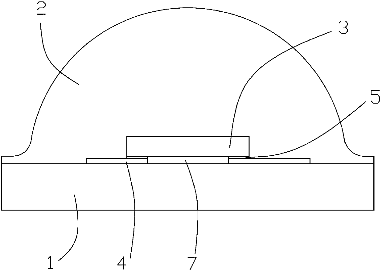
[0019] In this embodiment, a high-power ceramic LED wireless packaging structure, such as figure 1 As shown, there is a base 1, which is a ceramic base, and two eutectic electrode pads 4 are arranged on the base, such as figure 2 As shown, two pins 6 are arranged on the bottom of the base, and the two pins are positive pins and negative pins respectively, and two eutectic electrode pads are respectively connected to the two pins. A light-emitting chip 3 is arranged on the eutectic electrode pad, and the light-emitting chip is a high-power light-emitting chip. On both sides of the bottom of the light-emitting chip, a positive electrode terminal and a negative electrode terminal are drawn respectively, and the positive electrode terminal and the negative electrode terminal protrude from the bottom of the light-emitting chip. On the surface, there is a layer of tin gold layer 5 on the positive electrode terminal and the negative electrode terminal. The thickness of the tin gold ...


PUM


Abstract

The invention relates to a wireless packaging structure of a high-power ceramic LED (Light-emitting Diode). The invention resolves the problems that in the prior art, the LED lamp adopts the bonding wire process, so that the process cost and the material cost are increased; and the bonding wire electrode is arranged above a luminous chip, so that the luminous efficiency of the light-emitting chip is reduced. The LED comprises a base, two eutectic electrode bonding wire pads, the luminous chip, and a lampshade jet-molded on the base; an anode end and a cathode end are led from the two sides of the bottom of the luminous chip respectively; the luminous chip is arranged at the two eutectic electrode bonding pads; the anode end is connected with one eutectic electrode bonding pad; and the cathode end is connected with the other eutectic electrode bonding pad. The invention has advantages as follows: as the wireless packaging technology is used, the bonding wire process is reduced, the complexity of the technological process is reduced, the dependability of the semi-finished product production is improved, and the cost is saved; and because the bonding wire is not arranged over the luminous chip, the luminous efficiency of the luminous chip is improved.

Description

technical field [0001] The invention relates to an LED lamp, in particular to a high-power ceramic LED wireless packaging structure which reduces the complexity of the technological process, saves costs and improves the light output rate. Background technique [0002] The traditional ceramic high-power LED is to point the crystal-bonding silver glue on the position of the ceramic crystal-bonding pad first, and then bind the high-power chip on it. After the silver glue is completely cured, stick the high-power LED chip firmly on the ceramic solder pad. On the plate, then solder the wires, and finally complete the package. Because the traditional high-power LED is solidified by silver glue, when the high-power LED is working, the chip will generate a lot of heat. The heat needs to be conducted to the pad of the ceramic base through the silver glue, and then the heat will be transferred to The heat dissipation is done on the ceramic base. Due to the limited heat conduction of ...

Claims


Application Information

Patent Timeline
Patent Type & Authority Applications(China)
IPC IPC(8): H01L33/48H01L33/62
CPCH01L2224/16225H01L2924/181H01L2924/00012
Inventor 李革胜黎云汉连程杰
Owner ZHEJIANG INTELED OPTOELECTRONICS TECH
Why Eureka
Try Eureka