


Quick Research
Generate reliable direction feasibility study reports for your R&D in just a few steps.

Technical Q&A
Discover and master advanced knowledge NOW. Basics, ideas, possibilities, all at once.

Find Solutions
As an expert in R&D theories, this can generate solutions to your technical problems instantly.

Evaluate Feasibility
Analyze your overall solution with one click, know your potential R&D risks in advance.

Monitor Landscape
Get weekly tech updates, stay abreast of the latest tech innovations and key insights.
Semiconductor integrated circuit and receiving apparatus
A technology of integrated circuits and semiconductors, applied in electrical components, multi-terminal pair networks, transmission systems, etc., can solve problems such as difficult low-voltage operation, increased installation costs, and degradation of analog circuit noise characteristics
- Summary
- Abstract
- Description
- Claims
- Application Information
AI Technical Summary
Problems solved by technology
Method used
Image

Examples
no. 1 Embodiment
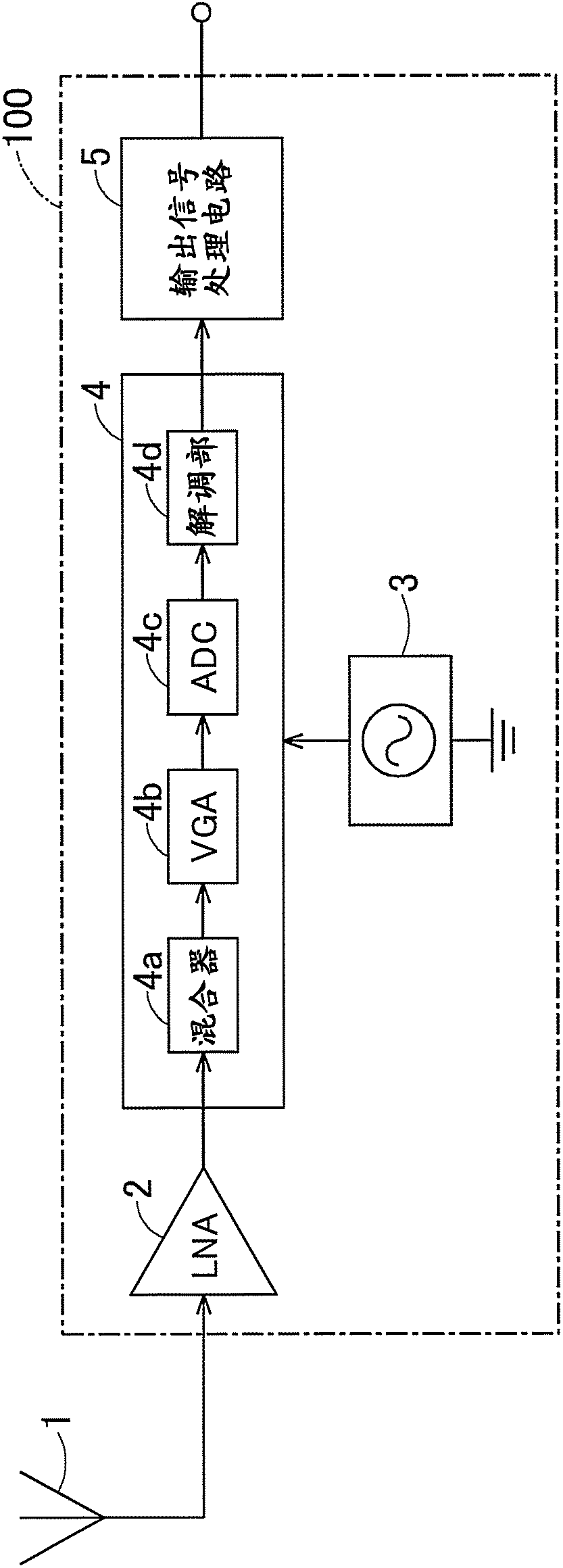
[0031] figure 1 It is a schematic block diagram of the receiving device 100 of the first embodiment. The receiving device 100 includes an LNA (semiconductor integrated circuit) 2 , an LO (Local Oscillator: local oscillator) signal generating unit 3 , a demodulation circuit 4 , and an output signal processing circuit 5 . The receiving device 100 is mounted on, for example, a wireless LAN (Local Area Network: Local Area Network) device, processes a radio wave signal received by the antenna 1 , and outputs it to the outside.
[0032] LNA2 amplifies the radio signal received by antenna 1 . The LO signal generator 3 generates an LO signal to be used as a reference for demodulating the radio wave signal. The frequency of the LO signal is, for example, 2.5 GHz. The demodulation circuit 4 demodulates the amplified radio wave signal based on the LO signal. More specifically, the demodulation circuit 4 has a mixer 4a, a VGA (Variable Gain Amplifier: variable gain amplifier) 4b, an...
no. 2 Embodiment
[0082] The first embodiment described above is provided with an impedance adjustment section whose impedance value is fixed. On the other hand, in the second embodiment described below, an impedance adjustment unit whose impedance is variable is provided.
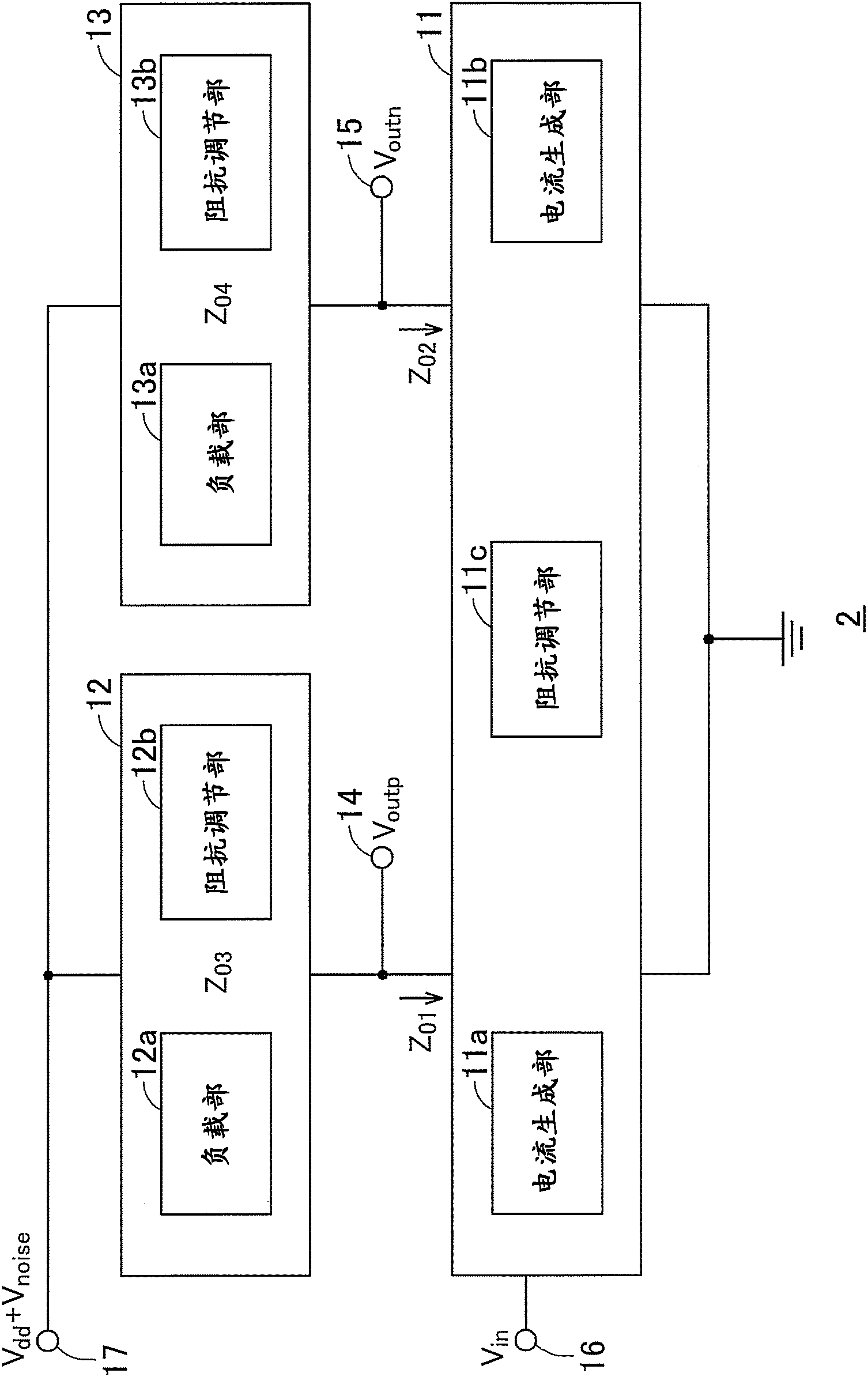
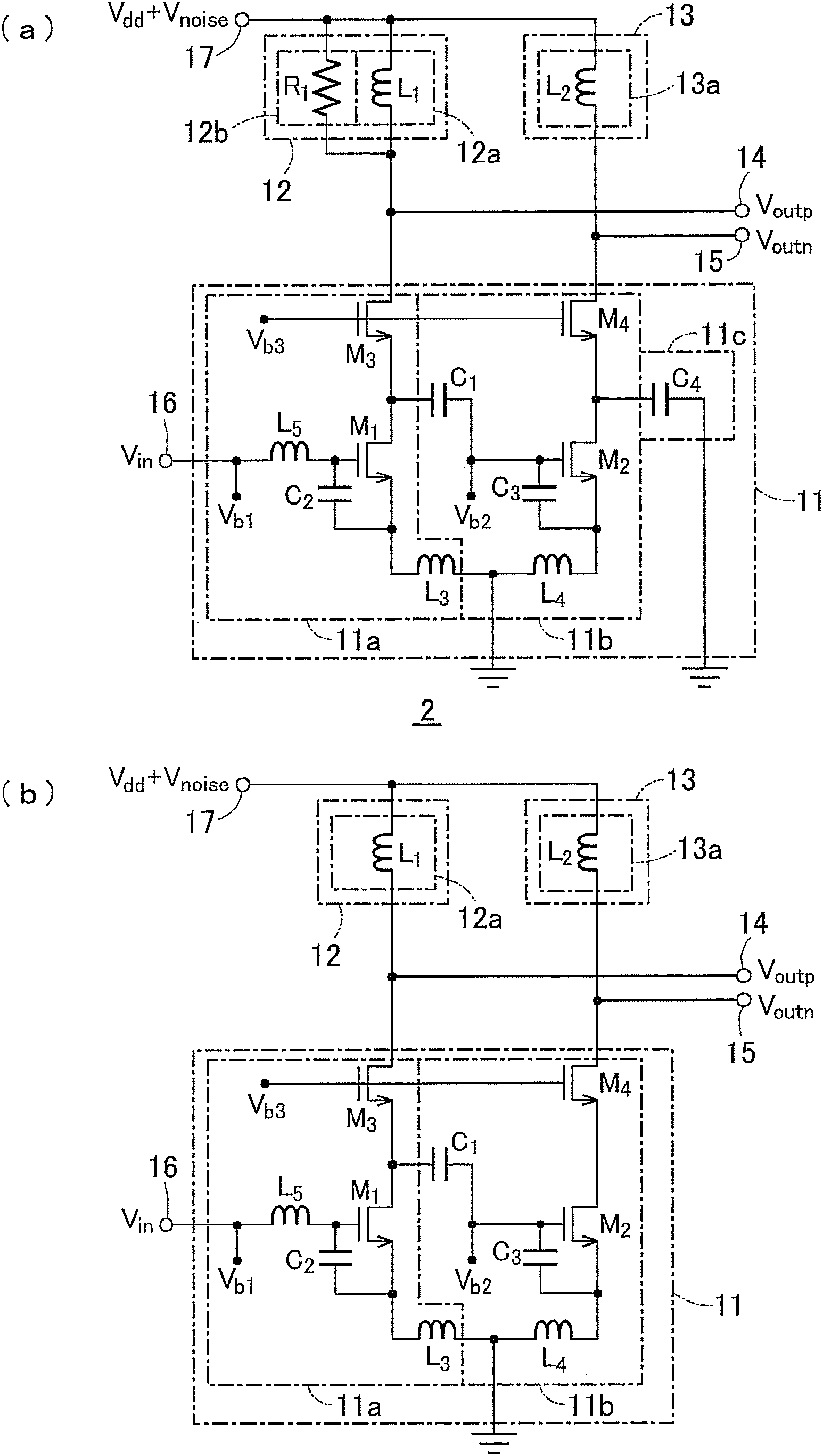
[0083] Figure 11 It is a schematic block diagram of an example of the internal configuration of the LNA 21 of the second embodiment. Figure 11 in, with figure 2 The same components are assigned the same symbols, and the following description will focus on the differences.
[0084] Control signals V1 to V3 are input to impedance adjustment units 111c, 121b, and 131b of LNA21, respectively. The impedances of the impedance adjustment parts 111c, 121b, and 131b can be variably controlled by the control signals V1 to V3. and figure 2 Similarly, at least one of the transconductance circuit 111 and the load circuits 121 and 131 only needs to have an impedance adjustment unit to which a control signal is input.
[0085] E...
no. 3 Embodiment
[0099] The third embodiment automatically sets the control signal in the second embodiment.
[0100] Figure 19 It is a schematic block diagram of the receiving device 101 of the third embodiment. Figure 19 in, with figure 1 The same components are attached with the same symbols, and the following description will focus on the differences.
[0101] Figure 19 The receiving device 101 further includes a detection circuit 6 and a control circuit 7 . Alternatively, LNA21 as Figure 11 As shown, there is at least one impedance adjustment part that variably controls the impedance according to the control signal. The detection circuit 6 detects degradation of the output signal of the output signal processing circuit 5 . The control circuit 7 sets the control signal of the LNA 21 so as to suppress the degradation of the output signal.
[0102] The control circuit 7 sets all the control signals to all values, for example, and finally sets the value in which the degradation of ...
PUM
 Abstract
Description
Claims
Application Information
 - R&D Engineer
- R&D Manager
- IP Professional
- Industry Leading Data Capabilities
- Powerful AI technology
- Patent DNA Extraction
Browse by: Latest US Patents, China's latest patents, Technical Efficacy Thesaurus, Application Domain, Technology Topic, Popular Technical Reports.
© 2024 PatSnap. All rights reserved.Legal|Privacy policy|Modern Slavery Act Transparency Statement|Sitemap|About US| Contact US: help@patsnap.com