Solid state imaging device, method of producing solid state imaging device, and electronic apparatus
A technology of solid-state imaging device and manufacturing method, which is applied in the direction of electric solid-state devices, radiation control devices, circuits, etc., can solve problems such as difficult design, and achieve the effect of increasing production and reducing changes
Active Publication Date: 2012-09-26
SONY CORP
View PDF5 Cites 30 Cited by
- Summary
- Abstract
- Description
- Claims
- Application Information
AI Technical Summary
Problems solved by technology
In such a structure, the transfer channel and the overflow channel are basically the same when transferring signal charges, so it is difficult to design
Method used
View moreImage
Smart ImageViewing Examples

Examples
no. 1 approach
[0034] 1. First Embodiment: Solid-state Imaging Device
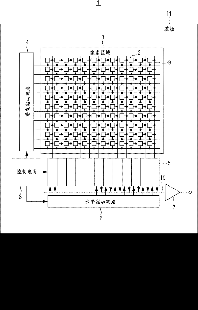
[0035] 1-1. Overall structure of solid-state imaging device
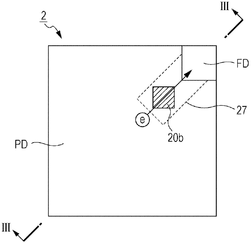
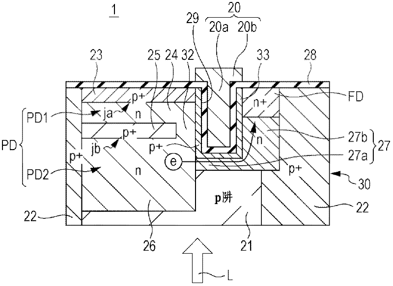
[0036] 1-2. Structure of main parts
[0037] 1-3. Manufacturing method
[0038] 1-4. Operation
[0039] 1-5. Modification 1
[0040] 1-6. Modification 2
no. 2 approach
[0041] 2. Second Embodiment: Manufacturing Method of Solid-State Imaging Device
no. 3 approach
[0042] 3. Third Embodiment: Manufacturing Method of Solid-State Imaging Device
Login to View More PUM
 Abstract
The invention discloses a solid state imaging device, a method of producing solid state imaging device, and an electronic apparatus. A solid state imaging device includes: a substrate; a photoelectric conversion unit that is formed on the substrate to generate and accumulate signal charges according to light quantity of incident light; a vertical transmission gate electrode that is formed to be embedded in a groove portion formed in a depth direction from one side face of the substrate according to a depth of the photoelectric conversion unit; and an overflow path that is formed on a bottom portion of the transmission gate to overflow the signal charges accumulated in the photoelectric conversion unit.
Description
[0001] Cross References to Related Applications [0002] This application contains subject matter related to that disclosed in Japanese Priority Patent Application JP 2011-063974 filed in the Japan Patent Office on Mar. 23, 2011, the entire content of which is hereby incorporated by reference. technical field [0003] The present invention relates to a solid-state imaging device having a vertical transistor, a method of manufacturing the solid-state imaging device, and electronic equipment provided with the solid-state imaging device. Background technique [0004] The solid-state imaging device is classified into an amplifying solid-state imaging device represented by a device such as a complementary metal oxide semiconductor (Complementary Metal Oxide Semiconductor, CMOS) image sensor, or a solid-state imaging device represented by a device such as a charge coupled device (Charge Coupled Device, CCD). The device is a representative charge transport type solid-state imaging ...
Claims
Login to View More Application Information
Patent Timeline
 IPC IPC(8): H01L27/146
CPCH01L27/14607H01L27/1461H01L27/14641H01L27/14656H01L27/14689H01L27/14612H01L27/14643H01L27/14614H01L27/14625H01L27/1464
Inventor 中村良助
Owner SONY CORP
Features
- R&D
- Intellectual Property
- Life Sciences
- Materials
- Tech Scout
- Unparalleled Data Quality
- Higher Quality Content
- 60% Fewer Hallucinations
Learn More Browse by: Latest US Patents, China's latest patents, Technical Efficacy Thesaurus, Application Domain, Technology Topic, Popular Technical Reports.
© 2025 PatSnap. All rights reserved.Legal|Privacy policy|Modern Slavery Act Transparency Statement|Sitemap|About US| Contact US: help@patsnap.com