Method for forming a decorative coating, a decorative coating, and uses of the same
A decorative, coating technology used in decorative coatings and forming decorative coatings, the method and field of application of decorative coatings, capable of addressing unfavorable, complex shapes of non-planar surfaces and poor ability of substrates and other problems, to achieve good thickness uniformity, prevent uneven color appearance, and promote the effect of optical design
- Summary
- Abstract
- Description
- Claims
- Application Information
AI Technical Summary
Problems solved by technology
Method used
Image
Examples
Embodiment 1
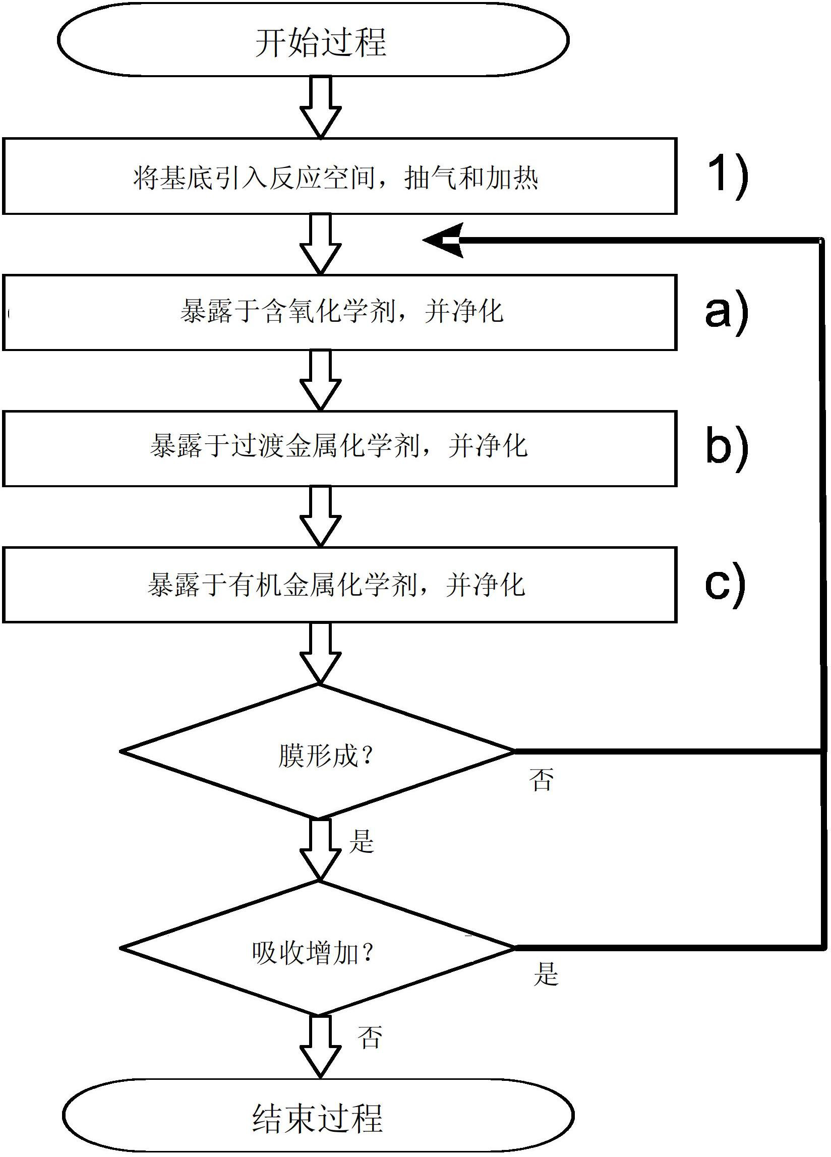
[0077] Using different processing temperatures, an absorbing film is formed on a substrate according to a first embodiment of the invention (see figure 1 ). First, a visually substantially transparent D263T glass substrate (available from Schott AG, Germany) with a thickness of 0.3 mm was inserted into the reaction space of a P400ALD batch processing unit (available from Beneq OY, Finland). The substrate is planar, enabling reliable light transmission measurements. The substrate is placed in the reaction space such that both sides of the substrate glass are exposed (ie not shaded) to the surrounding reaction space. In this embodiment, the above-mentioned carrier gas responsible for purifying the reaction space is nitrogen (N 2 ).
[0078] After the preparation of loading the substrate into the ALD device, the reaction space of the ALD device was evacuated to negative pressure, and the carrier gas was set to flow continuously to reach a processing pressure of about 1 mbar (1...
Embodiment 2
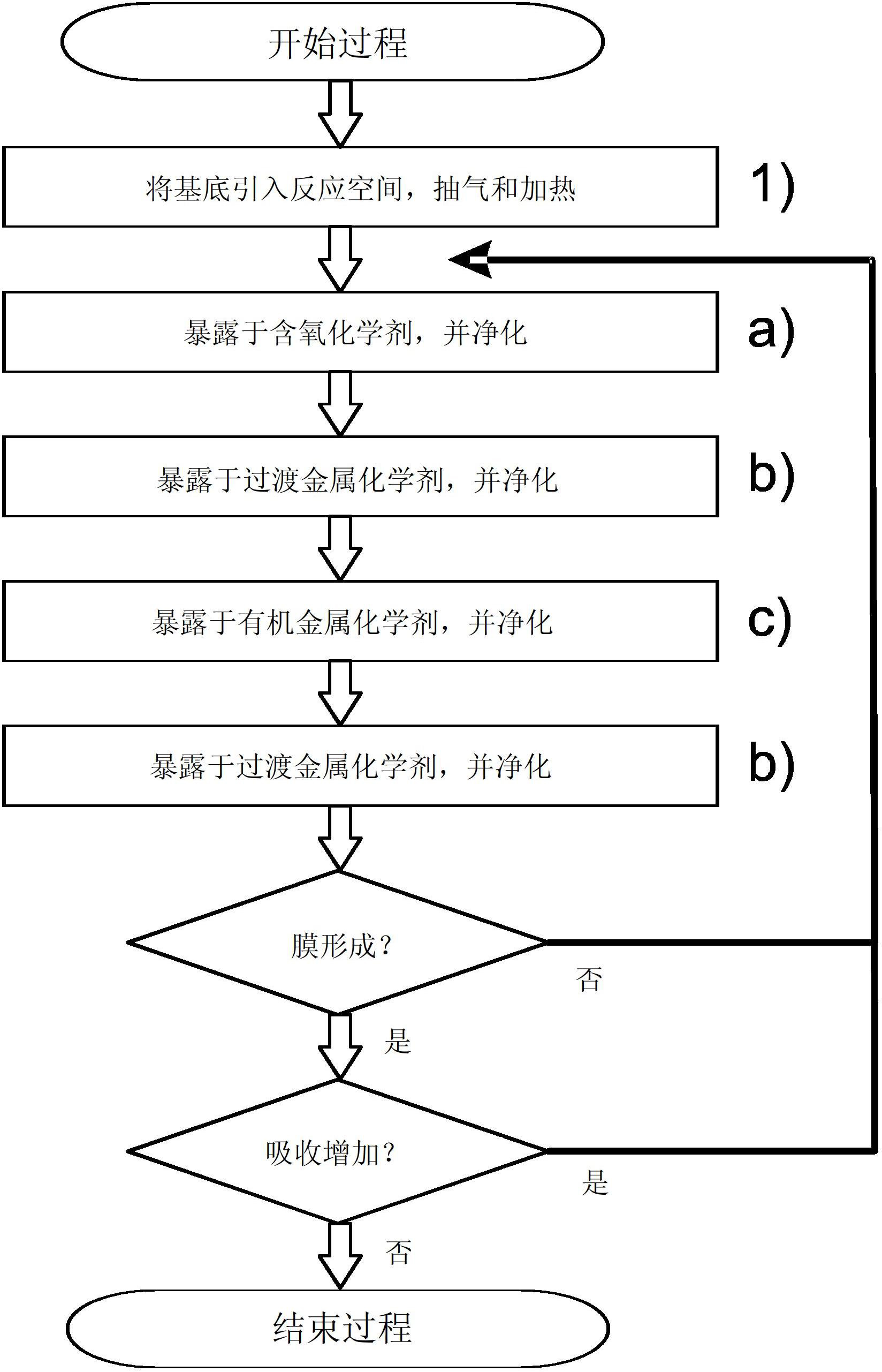
[0086] According to the second embodiment of the present invention, an absorbing film is formed on a substrate (see figure 2 ). First, a visually substantially transparent D263T glass substrate (available from Schott AG, Germany) with a thickness of 0.3 mm was inserted into the reaction space of a P400ALD batch processing unit (available from Beneq OY, Finland). The substrate is planar, enabling reliable light transmission measurements. The substrate is placed in the reaction space such that both sides of the substrate glass are exposed (ie not shaded) to the surrounding reaction space. In this embodiment, the above-mentioned carrier gas responsible for purifying the reaction space is nitrogen (N 2 ).
[0087] After the preparation of loading the substrate into the ALD device, the reaction space of the ALD device was evacuated to negative pressure, and the carrier gas was set to flow continuously to reach a processing pressure of about 1 mbar (1 hPa), followed by heating t...
PUM
| Property | Measurement | Unit |
|---|---|---|
| thickness | aaaaa | aaaaa |
Abstract
Description
Claims
Application Information
 - R&D Engineer
- R&D Manager
- IP Professional
- Industry Leading Data Capabilities
- Powerful AI technology
- Patent DNA Extraction
Browse by: Latest US Patents, China's latest patents, Technical Efficacy Thesaurus, Application Domain, Technology Topic, Popular Technical Reports.
© 2024 PatSnap. All rights reserved.Legal|Privacy policy|Modern Slavery Act Transparency Statement|Sitemap|About US| Contact US: help@patsnap.com


