
Array substrate and manufacturing method thereof

An array substrate and transparent substrate technology, applied in the field of display manufacturing, can solve the problems of difficult design of parasitic capacitance, fluctuation of light transmittance, reduction of aperture ratio, etc.

Active Publication Date: 2012-09-05
BOE TECH GRP CO LTD
View PDF5 Cites 10 Cited by
  • Summary
  • Abstract
  • Description
  • Claims
  • Application Information

AI Technical Summary

Problems solved by technology

[0005] The appearance of the induced voltage will cause the asymmetry of the driving voltage, resulting in the fluctuation of the light transmittance, causing low-frequency brightness changes and head shaking, that is, flickering
In order to reduce the influence of the induced voltage, a larger storage capacitor C is usually used st , but conventionally increases the storage capacitor C st The method, such as increasing the area of ​​the storage capacitor, will lead to a decrease in the aperture ratio
In addition, although it can be seen from the above formula that reducing the parasitic capacitance can also reduce the induced voltage, the design of reducing the parasitic capacitance by changing the overlapping area is difficult to realize due to the strict requirements on the specifications of thin-film transistors in the prior art

Method used


Image

  • Array substrate and manufacturing method thereof
  • Array substrate and manufacturing method thereof
  • Array substrate and manufacturing method thereof

Examples


Embodiment Construction

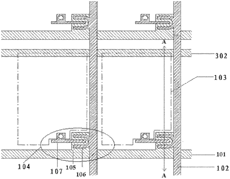
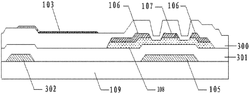
[0025] The following will clearly and completely describe the technical solutions in the embodiments of the present invention with reference to the accompanying drawings in the embodiments of the present invention. Obviously, the described embodiments are only some, not all, embodiments of the present invention. Based on the embodiments of the present invention, all other embodiments obtained by persons of ordinary skill in the art without making creative efforts belong to the protection scope of the present invention.

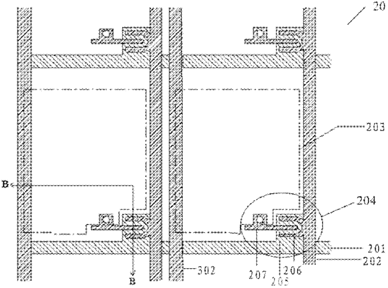
[0026] An array substrate provided by an embodiment of the present invention, for example, such as image 3 In the array substrate 20 shown, from a plan view, the source 206 of the thin film transistor 204 of the substrate is arc-shaped, and one end of the drain 207 is located at the centripetal side of the arc-shaped source 206 . The array substrate 20 includes:

[0027] A transparent substrate, on which gate lines 201 and data lines 202 intersecting horizon...


PUM


Abstract

The embodiment of the invention provides an array substrate and a manufacturing method thereof, which relate to the field of manufacturing of display elements and are used for reducing induced voltage of pixel electrodes to reduce screen flicker. The array substrate comprises a transparent substrate; grid lines and data lines crossed horizontally and longitudinally are arranged on the transparent substrate, and thin film transistors and the pixel electrodes are arranged in pixel units defined by the grid lines and the data lines; and grid electrodes of the thin film transistors are connected with the grid lines, source electrodes of the thin film transistors are connected with the data lines, and leakage electrodes of the thin film transistors are connected with the pixel electrodes. The array substrate is characterized in that the grid electrodes of the thin film transistors in an area just opposite to the leakage electrodes are thicker than that of the grid electrodes in an area just opposite to channels of the thin film transistors. The array substrate and the manufacturing method thereof are used in the field of manufacturing of the display elements.

Description

technical field [0001] The invention relates to the field of display manufacturing, in particular to an array substrate and a manufacturing method thereof. Background technique [0002] refer to figure 1 The top view of the array substrate shown and figure 2 As shown in the cross-sectional view of the A-A direction, the structure of the array substrate 10 in the prior art is: on the transparent substrate 109, gate lines and data lines intersecting horizontally and vertically are formed, and pixels defined by the gate lines and data lines A thin film transistor 104 and a pixel electrode 103 are arranged in the unit; wherein the thin film transistor 104 includes: a gate 105 , a source 106 and a drain 107 , and the drain 107 is electrically connected to the pixel electrode 103 through a via hole. From a top view, it can be seen that the gate 105 and the drain 107 have an overlapping area, which will generate a parasitic capacitance C gd . Due to the C of the drain 107 and ...

Claims


Application Information

Patent Timeline
IPC IPC(8): H01L27/12H01L21/77
CPCH01L27/124H01L29/42384
Inventor 朱佩誉牛菁
Owner BOE TECH GRP CO LTD
Learn More