
Liquid crystal display panel and manufacturing method and display device thereof

A liquid crystal display panel and display panel technology, which is applied in semiconductor/solid-state device manufacturing, instruments, electrical components, etc., can solve the problems of increasing the battery load of mobile phones, unfavorable display screen light and thin requirements, and large overlap deviation

Inactive Publication Date: 2012-09-05
BOE TECH GRP CO LTD +1
View PDF6 Cites 19 Cited by
  • Summary
  • Abstract
  • Description
  • Claims
  • Application Information

AI Technical Summary

Problems solved by technology

[0004] In the above-mentioned display structure, the inventors found that since the touch screen and the display screen are prepared separately, the formed touch screen generally has high cost, high thickness, and heavy weight, which is not conducive to the requirement of light and thin display screens; The overlap deviation during the bonding process is large, and the touch position cannot be accurately positioned; bonding the touch screen on the surface of the display will reduce the light transmittance of the display, and a higher power backlight is required under the same display brightness conditions. Further increases the load on the battery of the mobile phone, which is not conducive to the low power consumption requirements in the design of the mobile phone

Method used


Image

  • Liquid crystal display panel and manufacturing method and display device thereof
  • Liquid crystal display panel and manufacturing method and display device thereof
  • Liquid crystal display panel and manufacturing method and display device thereof

Examples


Embodiment 1

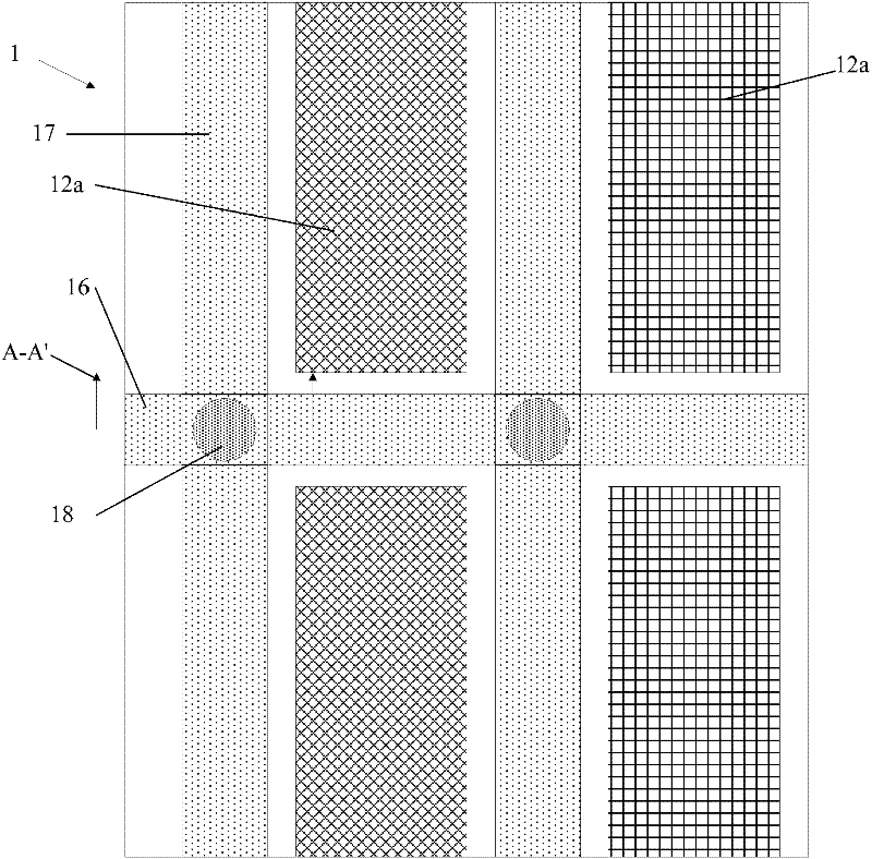
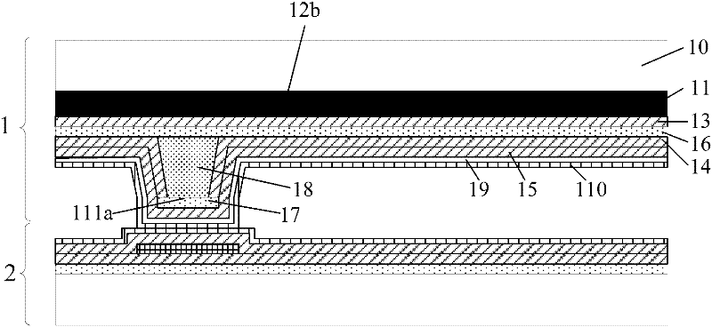
[0080] combine Figure 1A with 1B shown (where Figure 1A It is a schematic diagram of the top perspective structure of the color filter substrate of the liquid crystal display panel provided in Embodiment 1 of the present invention, Figure 1B Schematic diagram of the structure of the liquid crystal display panel provided by Embodiment 1 of the present invention at the section A-A of the color filter substrate), the liquid crystal display panel provided by the embodiment of the present invention includes a color filter substrate 1 and an array substrate 2, a color filter substrate 1 and an array substrate 2 is filled with liquid crystal (not shown in the figure), the color filter substrate 1 includes: a substrate 10; a color filter layer 11 formed on the substrate and a first insulating layer 13 covering the color filter layer 11, wherein the color filter layer includes The color filter pixel area 12a and the black matrix area 12b; the first conductive signal line 16 formed o...

Embodiment 2

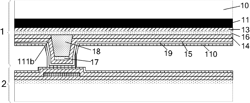
[0087] combine Figure 1C As shown (the schematic diagram of the top view perspective structure of the color filter substrate of the liquid crystal display panel provided by Embodiment 2 of the present invention is the same as that of Embodiment 1, refer to Figure 1A , Figure 1C Schematic diagram of the structure of the liquid crystal display panel provided by Embodiment 2 of the present invention at the section A-A of the color filter substrate), the liquid crystal display panel provided by the embodiment of the present invention includes a color filter substrate 1 and an array substrate 2, and a color filter substrate 1 and an array substrate 2 is filled with liquid crystal, and the color filter substrate 1 includes: a substrate 10; a color filter layer 11 formed on the substrate 10 and a first insulating layer 13 above the color filter layer 11, wherein the color filter layer 11 includes a color filter pixel area 12a and the black matrix region 12b; the first conductive s...

Embodiment 3

[0094] combine Figure 2A and 2B shown (where Figure 2A It is a schematic top view perspective structure diagram of the array substrate of the liquid crystal display panel provided by Embodiment 3 of the present invention, Figure 2B Schematic diagram of the structure of the liquid crystal display panel provided by Embodiment 3 of the present invention at the section A-A of the array substrate), the liquid crystal display panel provided by the embodiment of the present invention includes a color filter substrate 1 and an array substrate 2, and a color filter substrate 1 and an array substrate 2 Liquid crystals are filled between them, and the array substrate 2 includes: a substrate 20; data lines 24 and gate lines 21 that cross vertically and horizontally are formed on the substrate 20; pixel units and TFT switches are formed around the data lines 24 and gate lines 21, wherein the TFT The switch includes a gate electrode, a gate insulating layer 22, a source electrode, a dr...


PUM


Abstract

The embodiment of the invention provides a liquid crystal display panel and a manufacturing method and a display device thereof, and relates to the field of manufacturing of liquid crystal displays, wherein the thickness of a touch display panel can be reduced, and the touch precision and light transmittance can be improved. The display panel comprises a color-film substrate and an array substrate, wherein liquid crystal is filled between the color-film substrate and the array substrate; the color-film substrate comprises a substrate, a color-film layer, a first insulating layer, a first conductive signal wire, partition objects, a second insulating layer and a second conductive signal wire, wherein the color-film layer is on the substrate and the first insulating layer covers the color-film layer; the first conductive signal wire is on the first insulating layer; the partition objects are made of force sensitive resistance material and are evenly arranged on the first conductive signal wire; the second insulating layer covers the first conductive signal wire, the first insulating layer and the partition objects made of force sensitive resistance material; the second conductive signal wire is formed on the second insulating layer and intersected with the first conductive signal wire; and the second conductive signal wire passes through a through hole to be contacted with the other end of the partition object made of force sensitive resistance material. The embodiment of the invention is applied to manufacture of liquid crystal displays.

Description

technical field [0001] The invention relates to the field of liquid crystal display manufacturing, in particular to a liquid crystal display panel, a manufacturing method thereof, and a display device. Background technique [0002] As an optoelectronic product that integrates large-scale semiconductor integrated circuits and flat-panel light source technology with thin-film transistors as control elements and liquid crystals as the medium——thin-film transistor liquid crystal display has the advantages of low power consumption, portability, wide application range, and high quality. Become a new generation of mainstream display. [0003] In a display device, a touch panel is used in order to allow a user to perform related operations while viewing a screen. The touch display screen is one of the important carriers that integrate the input and output terminals; by measuring the coordinate position of the touch point on the display screen, the toucher's intention can be known a...

Claims


Application Information

Patent Timeline
IPC IPC(8): G02F1/1335G02F1/1339G02F1/1333G02F1/1362G02F1/1368H01L21/77
CPCG02F1/133G02F1/1339G06F3/0412G02F1/13394G06F3/04146
Inventor 李坤玄明花高永益
Owner BOE TECH GRP CO LTD
Learn More