


Quick Research
Generate reliable direction feasibility study reports for your R&D in just a few steps.

Technical Q&A
Discover and master advanced knowledge NOW. Basics, ideas, possibilities, all at once.

Find Solutions
As an expert in R&D theories, this can generate solutions to your technical problems instantly.

Evaluate Feasibility
Analyze your overall solution with one click, know your potential R&D risks in advance.

Monitor Landscape
Get weekly tech updates, stay abreast of the latest tech innovations and key insights.
Distributed feedback type organic semiconductor laser preparation method based on laser interferometer lithography
A laser interference lithography and distributed feedback technology, applied in the field of nanometer optoelectronic materials and devices, can solve the problems of complex process, expensive equipment, low efficiency, etc., and achieve the effects of good repeatability, high preparation efficiency and low cost
- Summary
- Abstract
- Description
- Claims
- Application Information
AI Technical Summary
Problems solved by technology
Method used
Image

Examples
Embodiment 1
[0018] Embodiment 1: Preparation of one-dimensional organic semiconductor nano-grating structure (one-dimensional structure)
[0019] 1) The recording medium S1805 photoresist is spin-coated on a glass substrate. The spin coating speed is 1800rpm, and the corresponding film thickness is 500nm;
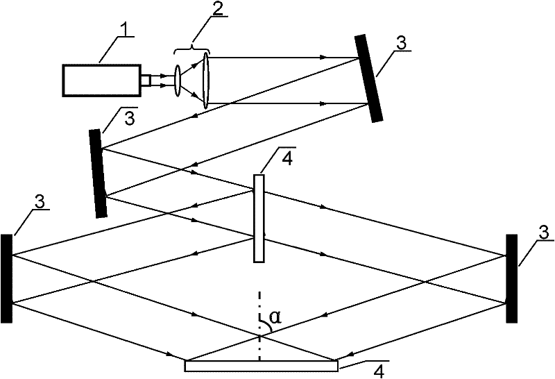
[0020] 2) Place the photoresist film sample prepared above in the interference optical path, such as figure 1 As shown, the angle between the two light beams α=22°, and the laser wavelength used for interference lithography is 355nm, the interference fringes can be recorded on the photoresist film, and then the photoresist sample is developed and fixed to obtain Periodic one-dimensional distributed feedback structure;
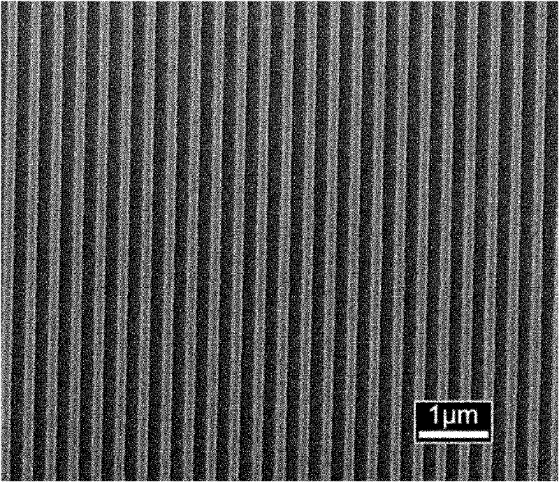
[0021] 3) The atomic force microscopy image of the prepared one-dimensional distributed feedback structure is as follows: figure 2 As shown, in the case of α=22°, the period of the prepared organic semiconductor grating is 355nm.
[0022] 4) Dissolving the organic ...
Embodiment 2
[0024] Embodiment 2: Preparation of two-dimensional distributed feedback structure (two-dimensional square structure)
[0025] On the basis of the one-dimensional distributed feedback structure preparation technology realized in Example 1, the sample is rotated 90° around its normal, and then the second interference exposure is performed to realize the preparation of the two-dimensional distributed feedback structure; and then The F8BT organic semiconductor solution is spin-coated on the distributed feedback structure of the recording medium to obtain a two-dimensional distributed feedback organic organic semiconductor laser.
Embodiment 3
[0026] Embodiment 3: Preparation of two-dimensional distributed feedback structure (two-dimensional triangular structure)
[0027] On the basis of the one-dimensional distributed feedback structure preparation technology realized in Example 1, the sample is rotated 60° around its normal, and then the second interference exposure is performed to realize the preparation of the two-dimensional distributed feedback structure; and then The F8BT organic semiconductor solution is spin-coated on the distributed feedback structure of the recording medium to obtain a two-dimensional distributed feedback organic organic semiconductor laser.
PUM
| Property | Measurement | Unit |
|---|---|---|
| Thickness | aaaaa | aaaaa |
| Wavelength | aaaaa | aaaaa |
Abstract
Description
Claims
Application Information
 - R&D Engineer
- R&D Manager
- IP Professional
- Industry Leading Data Capabilities
- Powerful AI technology
- Patent DNA Extraction
Browse by: Latest US Patents, China's latest patents, Technical Efficacy Thesaurus, Application Domain, Technology Topic, Popular Technical Reports.
© 2024 PatSnap. All rights reserved.Legal|Privacy policy|Modern Slavery Act Transparency Statement|Sitemap|About US| Contact US: help@patsnap.com