OLED (Organic Light Emitting Diode) pixel structure for compensating light emitting nonuniformity and driving method

A technology of pixel structure and light-emitting display device, which is applied in the direction of static indicators, instruments, etc., can solve the problems of non-uniform electrical performance, unsuitable for large-size panel application, uneven light emission, etc., and achieve the goal of eliminating non-uniformity of threshold voltage Effect

Active Publication Date: 2012-08-29
BOE TECH GRP CO LTD
View PDF6 Cites 25 Cited by
  • Summary
  • Abstract
  • Description
  • Claims
  • Application Information

AI Technical Summary

Problems solved by technology

Since the voltage of ARVDD is related to the current, IR Drop will also cause the current difference in different regions, and then produce mura when displaying
[0006] Third, the uneven film thickness of OLED devices will also cause non-uniformity in electrical properties during evaporation.
Figure 8 structure can compensate V TH The effects of non-uniformity, IR drop and OLED degradation, but because it is a current drive, it is not suitable for large-size panel applications
[0014] It can be seen that no effective means to solve the aforementioned technical problems has been proposed in the prior art, that is, how to solve the degradation of the OLED device, the non-uniformity of the threshold voltage of the TFT drive tube, and the luminescence caused by the voltage drop (IR drop) of the backplane power supply. Compensate for unevenness

Method used


Image

  • OLED (Organic Light Emitting Diode) pixel structure for compensating light emitting nonuniformity and driving method
  • OLED (Organic Light Emitting Diode) pixel structure for compensating light emitting nonuniformity and driving method
  • OLED (Organic Light Emitting Diode) pixel structure for compensating light emitting nonuniformity and driving method

Examples


Embodiment Construction

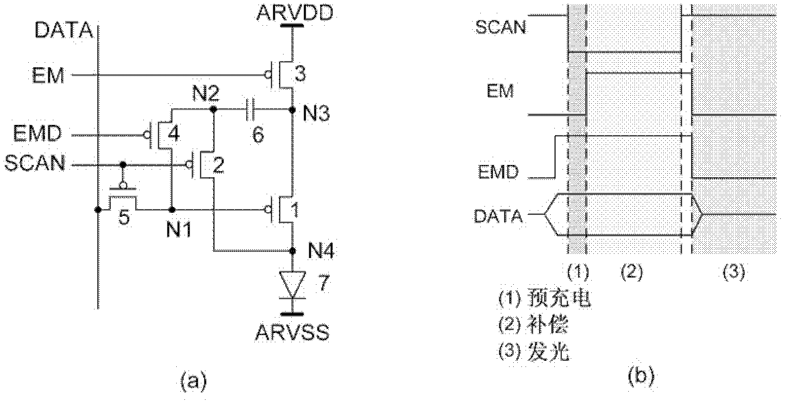
[0034] Such as figure 1 As shown in (a), the pixel circuit structure is composed of P-type TFT transistors 1 to 5, capacitor 6 and OLED 7, ARVDD and ARVSS are the backplane DC positive and negative levels respectively, DATA is the data voltage signal, and SCAN is the row scanning voltage Signals, EM and EMD are control signals, the pixel units in the same row share the SCAN and EM, EMD control signals, and the pixel units in the same column share the DATA data voltage signal. In the pixel circuit structure according to the present invention, the drain of the first TFT 1 is connected to the negative level of the backplane through the OLED device, the source of the first TFT 1 is connected to the drain of the third TFT 3, and the third The source of the thin film transistor 3 is connected to the positive level of the backplane, one end of the capacitor 6 is connected between the first thin film transistor 1 and the third thin film transistor 3 (N3), and the other end of the cap...


PUM


Abstract

The invention provides an organic light emitting display pixel structure and a driving method thereof. The pixel structure comprises first to fifth thin film transistors, a capacitor and an OLED (Organic Light Emitting Diode) device, wherein the width to length ratio of the first thin film transistor is set to compensate the brightness loss caused by degradation of the OLED device. According to the pixel structure, the following steps are performed in the process of refreshing each frame image: in a precharging period, a scan line and a first control signal (EM) have low levels, and a second control signal (EMD) has a high level; in a compensating period, the scan line has a low level, and the first control signal (EM) and the second control signal (EMD) have high levels; and in a light emitting period, the scan line has a high level, and the first control signal (EM) and the second control signal (EMD) have low levels.

Description

technical field [0001] The invention relates to a pixel structure of an organic light-emitting display device, which can compensate for the non-uniform luminescence caused by the degradation of the OLED device, the non-uniformity of the threshold voltage of the TFT drive tube, and the voltage drop (IRdrop) of the backplane power supply. The present invention also relates to a method for driving the above-mentioned pixel structure. Background technique [0002] Organic light-emitting display diodes (OLEDs), as a current-mode light-emitting device, have been increasingly used in high-performance displays. With the increase of the display size, the traditional passive matrix organic light emitting display device (Passive Matrix OLED) requires a shorter driving time of a single pixel, so it needs to increase the transient current and increase the power consumption. At the same time, the application of high current will cause the voltage drop on the ITO line to be too large, and...

Claims


Application Information

Patent Timeline
Patent Type & Authority Applications(China)
IPC IPC(8): G09G3/32
CPCG09G3/3233G09G2300/0819G09G2300/0842G09G2300/0861G09G2320/0223G09G2320/043G09G3/02G09G2300/0866
Inventor 吴仲远
Owner BOE TECH GRP CO LTD
Why Eureka
Try Eureka