
Method for extracting and calculating capacitance parameter based on random walk in integrated circuit design

An integrated circuit and parameter extraction technology, which is applied in calculation, electrical digital data processing, special data processing applications, etc., can solve the problems of no further optimization of weight, slow calculation rate, and large memory consumption

Inactive Publication Date: 2012-08-29
TSINGHUA UNIV
View PDF3 Cites 25 Cited by
  • Summary
  • Abstract
  • Description
  • Claims
  • Application Information

AI Technical Summary

Problems solved by technology

Among them, a method is proposed to pre-calculate the data information required in the random walk algorithm under the condition of a given integrated circuit process, such as adding the transition probability distribution of the transfer area of ​​the two dielectric layers, and the corresponding weight distribution data, and apply it to the random walk In the algorithm, it solves the problem of slow calculation rate or large memory consumption of the current similar algorithms in the case of multi-layer media
Through observation, it is found that this algorithm and other similar algorithms do not further optimize the weights and sampling methods used in the Monte Carlo process involved in the random walk algorithm, resulting in low algorithm efficiency.

Method used


Image

  • Method for extracting and calculating capacitance parameter based on random walk in integrated circuit design
  • Method for extracting and calculating capacitance parameter based on random walk in integrated circuit design
  • Method for extracting and calculating capacitance parameter based on random walk in integrated circuit design

Examples


Embodiment Construction

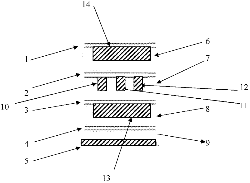
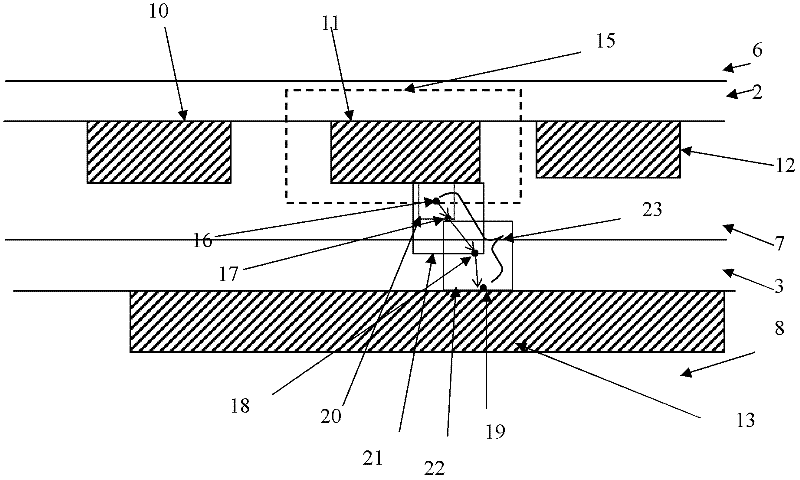
[0056] The database building and importance sampling processing of the present invention have been realized by MATLAB programming, and the FRW has been realized by C++ language programming, which can run on the LINUX operating system on the Intel workstation and the Linux operating system on the PC. Below in conjunction with a specific embodiment, the capacitance extraction process containing the importance sampling library construction process method is illustrated, so as to figure 1 For implementing an example, respectively place a long wire at the place of the long wire 10,11,12, respectively place 19 short wires at the place of the long wire 13 and 14, and intersect with the direction of the long wire 10,11,12 in a horizontal plane.

[0057] (1) Set the dielectric constant combination of the interface between two adjacent dielectric layers in the integrated circuit as (ε - =2.6,ε + =5), n=5 (in order to facilitate layout writing, set n=5 to be known, in order to ensure a...


PUM


Abstract

The invention relates to a method for extracting and calculating a capacitance parameter based on a random walk in an integrated circuit design, belonging to the technical field of integrated circuit computer aided designs, and comprising the following steps of: (1) setting the combination of the upper and lower dielectric constants of each interface in an integrated circuit and setting up a cubic transition area model, obtaining the relationship between the potential of an area surface grid and a central potential by a numerical way and taking the relationship as an initial transition probability intensity vector, and converting the initial transition probability intensity vector into a transition intensity vector and a corresponding weight numerical vector according to an importance collecting idea, and then processing and storing the transition intensity vector and the corresponding weight numerical vector into a database; and (2) correspondingly modifying a weight sampling way and a weight numerical value in a random walk algorithm by the data calculated in Step (1), and extracting and calculating the capacitance parameter in the integrated circuit. The random walk sampling weight numerical value generated by the method is unified, and the sampling probability tends to a location contributing great to the Gauss surface integral. The method for extracting and calculating the capacitance parameter has higher calculating efficiency and the design period for the integrated circuit is shortened.

Description

technical field [0001] The invention relates to a method for extracting and calculating capacitance parameters based on random walk in integrated circuit design, and belongs to the technical field of integrated circuit computer aided design. Background technique [0002] In the design process of an integrated circuit, a functional description must first be proposed, and then a layout describing the size and structure of the semiconductor process is obtained through logic design and layout design. At this time, "layout verification" is required, that is, to verify whether the above-mentioned design can meet the originally set requirements through computer software simulation. If the requirements are met, the next step of production and manufacturing can be carried out; otherwise, it is necessary to return to logic design and make necessary corrections. This iterative process is repeated until layout verification shows that the design does meet the requirements. In layout ve...

Claims


Application Information

Patent Timeline
Patent Type & Authority Applications(China)
IPC IPC(8): G06F17/50
Inventor 喻文健庄昊
Owner TSINGHUA UNIV
Learn More