
Jogging element-based infrared detector for modulating GaN HEMT channel current

An infrared detector and channel current technology, applied in the field of infrared detectors, can solve the problems of unfavorable integration of reference optical paths, electrochemical corrosion, difficult process and high cost

Active Publication Date: 2012-08-15
BEIJING UNIV OF TECH
View PDF4 Cites 2 Cited by
  • Summary
  • Abstract
  • Description
  • Claims
  • Application Information

AI Technical Summary

Problems solved by technology

Question 1: If attached figure 1 As shown, it is a high-sensitivity, uncooled tunneling infrared sensor based on the micro-mechanical displacement of the electron tunneling mechanism, but the structure of this detector is complicated, the process is difficult and the cost is high
Although Kaoru Yamashita et al. directly used air as the infrared absorption medium and adopted the microcapacitance detection method on this basis, which greatly reduced the process difficulty of device preparation, but also reduced the detection rate at the same time.
Question 2: In addition to this, other research groups have also proposed SiN x A double cantilever beam MIRROR infrared detection system composed of Au and Au, but the existence of the reference optical path of the system is not conducive to integration
Question 3: Detectors based on diode current-voltage temperature characteristics need to be electrochemically corroded, which increases the array area and increases the complexity of the array design

Method used


Image

  • Jogging element-based infrared detector for modulating GaN HEMT channel current
  • Jogging element-based infrared detector for modulating GaN HEMT channel current

Examples


Embodiment 1

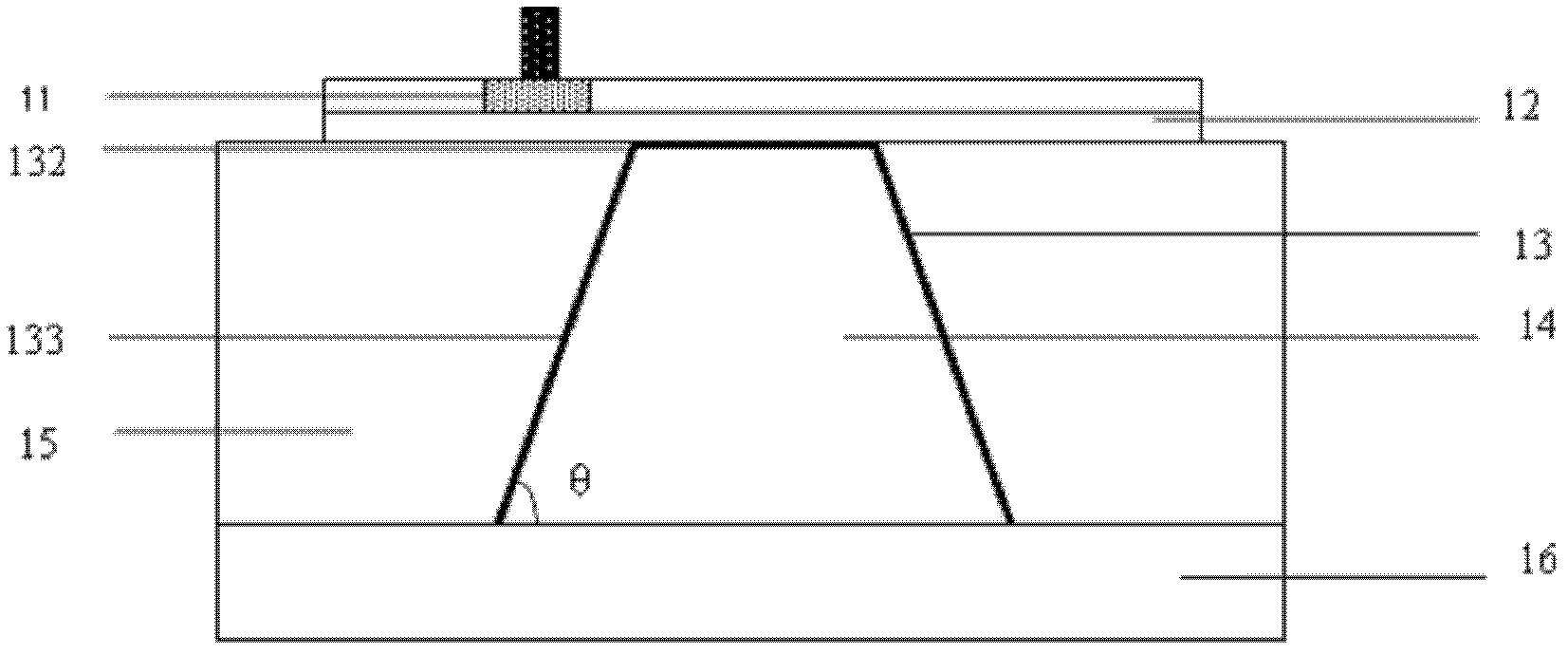
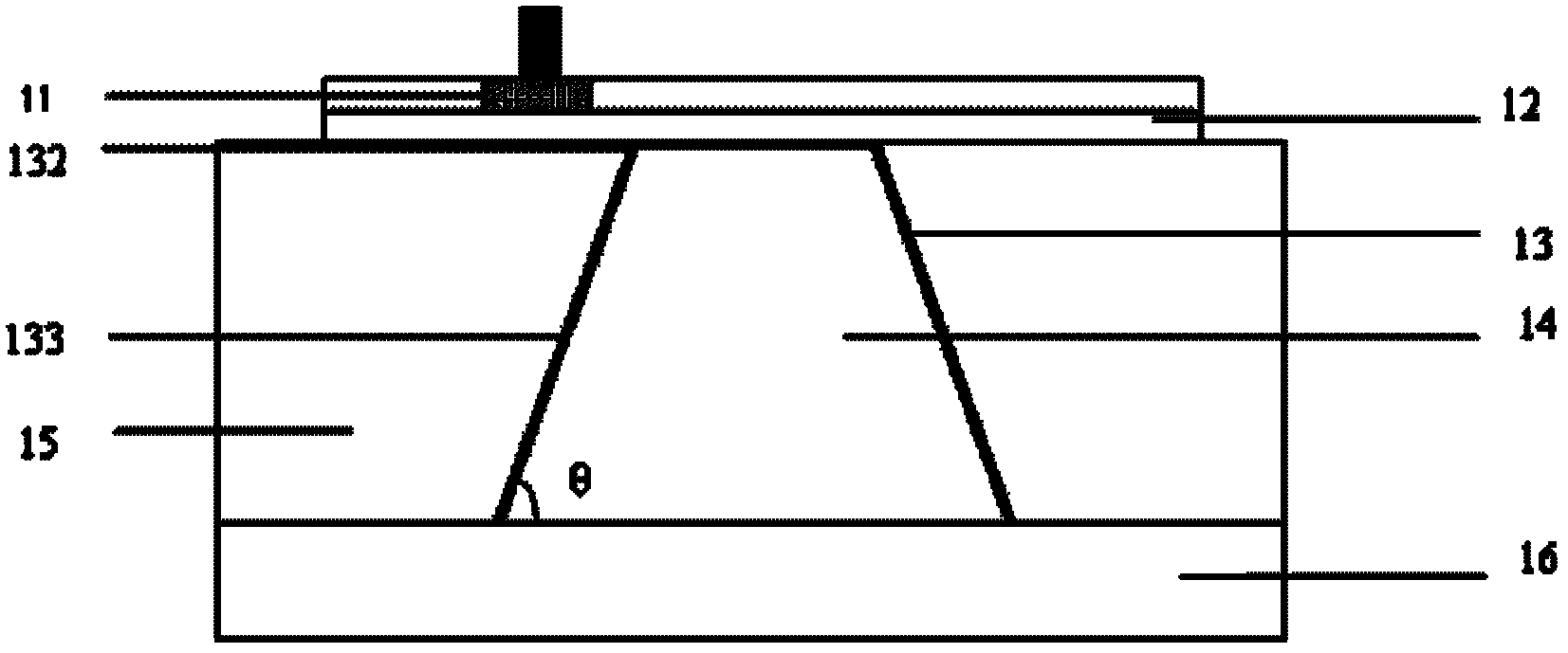
[0020] GaN / AlGaN HEMT is used as the HEMT device, Al is used as the infrared reflection layer in the light wave absorption auxiliary layer, and SiN x For the energy-absorbing film, the inclination angle θ of the prism gas-filled cavity is 45° as an example. The device consists of the following parts: GaN / AlGaN HEMT device, micro-moving element, light-wave absorption auxiliary layer, gas-filled cavity, substrate, absorbing light wave gas, A vertical GaN-based force-electrically coupled infrared detector composed of a window layer. The preparation process is as follows:

[0021] 1. First use the diffusion deposition process in Si / Al with GaN / AlGaN structure 2 O 3 The sheet forms a heterojunction to prepare a GaN / AlGaN heterojunction HEMT. For the Si substrate epitaxial GaN method, it is necessary to etch Si to leave the GaN / AlGaN diaphragm and HEMT; if Al is used 2 O 3 Substrate epitaxial GaN / AlGaN, you need to remove Al by polishing and ICP etching 2 O 3 Substrate.

[0022] 2. Usin...

Embodiment 2

[0026] GaN / AlGaN HEMT is used as the HEMT device, Ag is used as the infrared reflection layer in the light wave absorption auxiliary layer, and SiN x For the energy-absorbing film, the inclination angle θ of the prism gas-filled cavity is 45° as an example. The device consists of the following parts: GaN / AlGaN HEMT device, micro-moving element, light-wave absorption auxiliary layer, gas-filled cavity, substrate, absorbing light wave gas, A vertical GaN-based force-electrically coupled infrared detector composed of a window layer. The preparation process is as follows:

[0027] 1. First use the diffusion deposition process in Si / Al with GaN / AlGaN structure 2 O 3 The sheet forms a heterojunction to prepare a GaN / AlGaN heterojunction HEMT. For the Si substrate epitaxial GaN method, it is necessary to etch Si to leave the GaN / AlGaN diaphragm and HEMT; if Al is used 2 O 3 Substrate epitaxial GaN / AlGaN, you need to remove Al by polishing and ICP etching 2 O 3 Substrate.

[0028] 2. Usin...

Embodiment 3

[0032] GaN / AlGaN HEMT is used as the HEMT device, Al is used as the infrared reflection layer in the light wave absorption auxiliary layer, and SiN x For the energy-absorbing film, take the round-table gas-filled cavity as an example. The device consists of the following parts: GaN / AlGaN HEMT device, micro-movement element, light-wave absorption auxiliary layer, gas-filled cavity, substrate, light-wave gas absorption, vertical type window layer GaN-based force-electrically coupled infrared detector. The preparation process is as follows:

[0033] 1. First use the diffusion deposition process in Si / Al with GaN / AlGaN structure 2 O 3 The sheet forms a heterojunction to prepare a GaN / AlGaN heterojunction HEMT. For the Si substrate epitaxial GaN method, it is necessary to etch Si to leave the GaN / AlGaN diaphragm and HEMT; if using Al 2 O 3 Substrate epitaxial GaN / AlGaN, you need to remove Al by polishing and ICP etching 2 O 3 Substrate.

[0034] 2. Using MEMS technology to form a micro...


PUM


Abstract

The invention is used in the technical field of semiconductor photoelectron information, specifically relates to a jogging element-based infrared detector for modulating GaN HEMT (High Electron Mobility Transistor) channel current. The infrared detector is characterized by orderly comprising a GaN / AlGan HEMT device, a jogging element, a light wave absorption auxiliary layer, a gas-filled chamber, a substrate, a light wave absorption gas and a window layer. The jogging element is connected with the HEMT channel, after the light wave absorption gas in the gas-filled chamber and the light wave absorption auxiliary layer absorb the light wave, the gas-filled chamber deforms, the deformation drives the jogging element to move, and the movement of the jogging element induces the variation of the GaN HEMT channel current, thus, a light wave signal is converted into an electric signal to be detected. According to the invention, high sensitivity and high reliability of a GaN-based electro-mechanical coupling infrared detector are realized.

Description

Technical field [0001] The invention is used in the field of semiconductor optoelectronic information technology, and specifically relates to an infrared detector based on micro-movement elements modulating GaN HEMT (gallium nitride high electron mobility transistor) channel current. Background technique [0002] At present, the preferred development direction of thermal detector infrared detectors is that they can work at room temperature, have high detection rate, high response speed, wavelength selectivity, high reliability, and integrated arrays. At present, a series of pressure sensors have been proposed internationally. Although the structures of resistive, capacitive and conventional FET signal conversion infrared detectors have made great progress in a certain range, there are still problems in each structure. Question 1: As attached figure 1 As shown, it is a high-sensitivity, non-refrigerated tunneling infrared sensor based on the micromechanical displacement of the el...

Claims


Application Information

Patent Timeline
Patent Type & Authority Applications(China)
IPC IPC(8): G01J1/42
Inventor 朱彦旭曹伟伟郭伟玲徐晨
Owner BEIJING UNIV OF TECH
Learn More