
Package carrier and manufacturing method thereof

A technique for encapsulating a carrier board and a manufacturing method, which is applied in the fields of circuit heating devices, semiconductor/solid-state device manufacturing, printed circuits, etc., and can solve problems such as reduced reliability, shortened service life, and permanent damage of light-emitting diode chips and the encapsulation carrier board , to improve the use efficiency and service life, increase the thermal conductivity, best thermal conductivity and structural strength

Active Publication Date: 2012-08-08
SUBTRON TECH
View PDF3 Cites 11 Cited by
  • Summary
  • Abstract
  • Description
  • Claims
  • Application Information

AI Technical Summary

Problems solved by technology

In this way, the light-emitting diode chip may cause brightness attenuation and shorten service life due to overheating, and even cause permanent damage in severe cases
[0004] As the integration of integrated circuits increases, due to the thermal expansion coefficient mismatch between the LED chip and the package substrate, thermal stress and warpage are also increasingly occurring. Serious, and this result will lead to a decrease in the reliability (reliability) between the LED chip and the packaging substrate

Method used


Image

  • Package carrier and manufacturing method thereof
  • Package carrier and manufacturing method thereof
  • Package carrier and manufacturing method thereof

Examples


Embodiment Construction

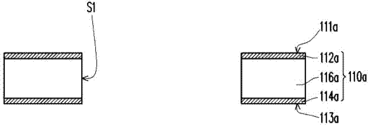
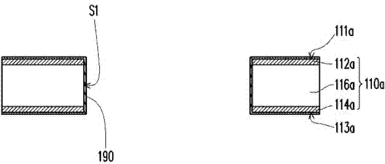
[0048] Figure 1A to Figure 1H It is a schematic cross-sectional view of a manufacturing method of a packaging carrier according to an embodiment of the present invention. Please refer to Figure 1A According to the manufacturing method of the packaging carrier of this embodiment, firstly, a substrate 110a is provided, wherein the substrate 110a has an upper surface 111a and a lower surface 113a opposite to the upper surface 111a. In this embodiment, the substrate 110a is composed of, for example, a first copper foil layer 112a, a second copper foil layer 114a, and a core dielectric layer 116a, wherein the core dielectric layer 116a is disposed on the first copper foil layer 112a and the second copper foil layer 114a. That is to say, the substrate 110a of this embodiment is a double-sided board.

[0049] Next, please refer to Figure 1B , forming a first opening S1 connecting the upper surface 111a and the lower surface 113a of the substrate 110a, wherein the first opening ...


PUM


Abstract

A manufacturing method of a package carrier is provided. A first opening communicating an upper surface and a lower surface of a substrate is formed. A heat-conducting element having a top surface and a bottom surface is configured in the first opening and fixed into the first opening via an insulation material. A first insulation layer and a first metal layer are laminated onto the upper surface. A second insulation layer and a second metal layer are laminated onto the lower surface. A second opening and a third opening respectively exposing portions of the top and the bottom surfaces are formed. At least one through via passing through the first metal layer, the first insulation layer, the substrate, the second insulation layer and the second metal layer is formed. A third metal layer covering the first and second metal layers and an inner wall of the through via is formed.

Description

technical field [0001] The present invention relates to a semiconductor structure and its manufacturing method, and in particular to a packaging carrier and its manufacturing method. Background technique [0002] The purpose of chip packaging is to protect the bare chip, reduce the density of chip contacts and provide good heat dissipation for the chip. Traditional wire bonding technology usually uses a leadframe as a chip carrier. As the chip's contact density gradually increases, the lead frame can no longer provide a higher contact density, so it can be replaced by a package substrate with a high contact density, and through metal wires or bumps, etc. The conductive medium is used to package the chip on the packaging substrate. [0003] Taking the currently commonly used LED packaging structure as an example, the LED chip needs to be packaged before use, and the LED chip will generate a large amount of heat energy when emitting light. If the heat energy generated by th...

Claims


Application Information

Patent Timeline
Patent Type & Authority Applications(China)
IPC IPC(8): H01L21/48H01L21/60H01L23/34H01L23/485H01L23/12
CPCH01L33/642H01L24/45H01L2924/15153H01L2224/73265H05K1/0204H05K2201/10106H01L2224/48235H01L2924/12041H01L23/3677H01L33/486H01L2224/45099H01L2224/48091H01L2924/01019H01L2224/48227H01L2924/00014H01L24/48H01L23/49827H01L2924/181H01L2924/00H01L2924/00012
Inventor 孙世豪
Owner SUBTRON TECH
Learn More