Ultra-narrow bandwidth dual-band filter based on asymmetric step impedance resonator
A step impedance and resonator technology, applied in the field of ultra-narrowband dual-frequency filter, can solve the problems of high attenuation, microstrip dual-frequency filter can not achieve good frequency selection characteristics, large size, etc., to achieve high frequency selection characteristics , with the effect of low interpolation loss and small size
- Summary
- Abstract
- Description
- Claims
- Application Information
AI Technical Summary
Problems solved by technology
Method used
Image
Examples
Embodiment 1
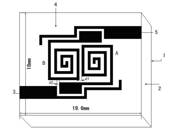
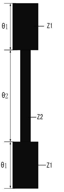
[0029] see figure 1 , the asymmetric step impedance ultra-narrow-band dual-band filter, comprising a dielectric substrate (2), a microstrip line (4) on the surface of the dielectric substrate (2), and a grounded metal coating (1) on the lower surface of the dielectric substrate; it is characterized in that The microstrip line (4) on the upper surface of the dielectric substrate is composed of two identical asymmetric step impedance resonators (A, B) and input and output feeders (3, 5); resonator A and resonator B are folded into a spiral structure, and are weakly coupled to each other; at the same time, the input and output feeders (3, 5) are also coupled and fed to the resonators (A, B) respectively.
Embodiment 2
[0031] This embodiment is basically the same as Embodiment 1, and the special features are as follows:
[0032] The length of each resonator (A, B) is one-half wavelength at the first center frequency, and both ends of each resonator (A, B) are open-circuited.
[0033] The input feeder and the output feeder (A, B) feed at 180 degrees.
[0034] The material of the microstrip line (4) and the ground metal plating layer (1) on the surface of the dielectric substrate (2) is gold, silver or copper with good electrical conductivity.
[0035] The dielectric substrate (2) has a dielectric constant of =2.65 of the dielectric board, the thickness of the dielectric board h =0.8mm.
Embodiment 3
[0037] Such as figure 1 Shown is the structure diagram of the ultra-narrowband dual-band filter based on the asymmetric step impedance resonator of this embodiment. The mutual coupling between resonator A and resonator B can generate two transmission zeros. At the same time, the position of the transmission zero point and the passband characteristics can be changed by adjusting the distance between the resonators. After design, simulation and optimization, the specific size of the microstrip ultra-narrowband dual-band filter is finally determined as follows:
[0038] L1=3.6mm, L2=5mm, L3=5.6mm, L4=5mm, L5=4.2mm, L6=3.2mm, L7=4mm,
[0039] L8=2.6 mm, L9=2.2 mm, L10=2 mm, L11=1.6 mm, L12=1.2 mm, L13=0.6 mm, L14=6 mm, L15=4.8 mm, L16=6.8 mm, W1=1.8 mm, W2=0.4 mm, W3=2 mm,
[0040] d1=d2=0.4 mm.
[0041] Based on the above method, a dual-band filter for wireless local area network (WLAN) is designed. Its center frequency is 2.4GHz / 5.22GHz, and the corresponding relative bandw...
PUM
 Abstract
Description
Claims
Application Information
 - R&D
- Intellectual Property
- Life Sciences
- Materials
- Tech Scout
- Unparalleled Data Quality
- Higher Quality Content
- 60% Fewer Hallucinations
Browse by: Latest US Patents, China's latest patents, Technical Efficacy Thesaurus, Application Domain, Technology Topic, Popular Technical Reports.
© 2025 PatSnap. All rights reserved.Legal|Privacy policy|Modern Slavery Act Transparency Statement|Sitemap|About US| Contact US: help@patsnap.com


