
Test method generated by monitoring negative bias temperature instability (NBTI) effect interface states in real time

A test method and real-time monitoring technology, applied in the direction of single semiconductor device testing, etc., can solve the problems of NBTI degradation recovery, inaccurate analysis of NBTI degradation mechanism, etc., and achieve the effect of reducing the amount of recovery

Active Publication Date: 2012-08-01
PEKING UNIV
View PDF2 Cites 16 Cited by
  • Summary
  • Abstract
  • Description
  • Claims
  • Application Information

AI Technical Summary

Problems solved by technology

However, in general semiconductor testers, the DC signal and pulse signal generation modules are different. After NBT (Negative Bias Temperature) stress is applied, the signal source module needs to be replaced to measure the charge pump current, which will cause a certain NBTI degradation and recovery, resulting in NBTI degradation mechanism analysis is inaccurate

Method used

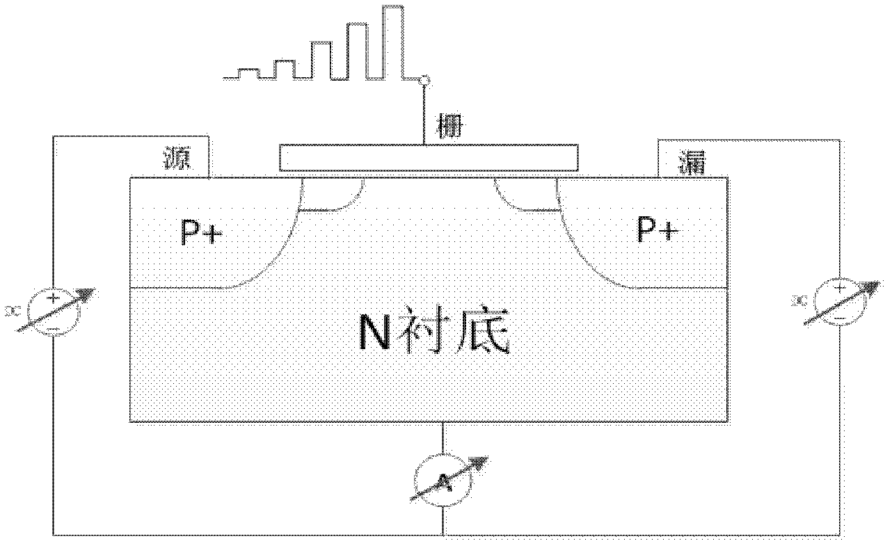
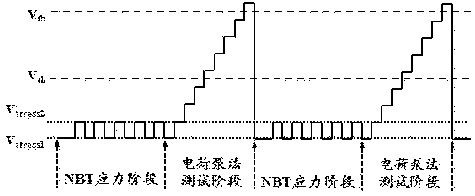
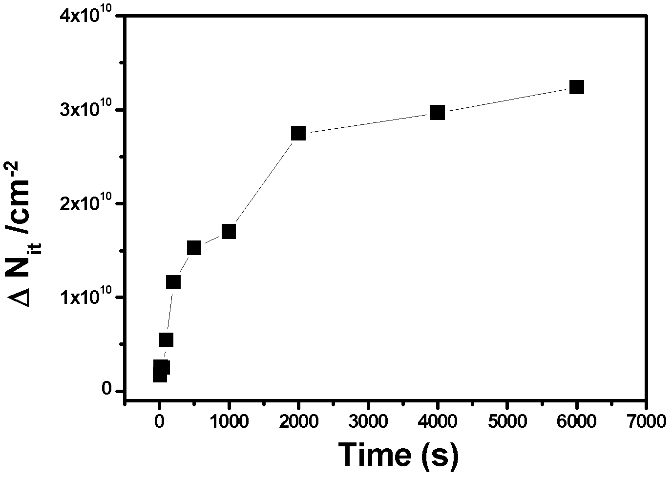

Image

  • Test method generated by monitoring negative bias temperature instability (NBTI) effect interface states in real time
  • Test method generated by monitoring negative bias temperature instability (NBTI) effect interface states in real time
  • Test method generated by monitoring negative bias temperature instability (NBTI) effect interface states in real time

Examples


Embodiment Construction

[0018] The preferred embodiment of the present invention is described in more detail below with reference to the accompanying drawings of the present invention.

[0019] In the embodiment of the auxiliary invention, the tested PMOS tube width (W) and length (L) are 5um and 0.18um respectively. NBTI stress bias is gate terminal pulse voltage high voltage is -2.55V, low voltage is -2.65V, frequency is 2MHz, and other terminals (source terminal, source terminal and substrate) are all grounded. At the same time, the charge pump test adopts the fixed low level method, the low level voltage is -2.55V, and the maximum high level voltage is 1V. During the application of NBT stress, the NBT stress was interrupted at t=10s, 20s, 50s, 100s, 200s, 500s, 1000s, 2000s, 4000s, 6000s, respectively, and the charge pump collected from the device substrate was quickly monitored by the charge pump test method Current I cp , and then use formula 1 to get the interface state charge generated afte...


PUM


Abstract

The invention discloses a test method generated by monitoring a negative bias temperature instability (NBTI) effect interface states in real time, which belongs to the field of reliable testing of semiconductor devices. The method enables a direct voltage signal source at negative bias temperature (NBT) stress polarization middle gate end to be changed into a pulse signal source, adopts a charge pump method to measure current on a substrate after NBT stress with different time, and immediately monitors increase of interface state charge caused by the NBTI effect. Compared with commonly-used test method of monitoring interface state charge changes, the test method has instantaneity, reduces recovery amount of NBTI degeneration, and can effectively assess influences of the NBTI effect on characteristics of devices.

Description

technical field [0001] The invention relates to the field of reliability testing of semiconductor devices, in particular, the NBTI effect of a PMOS device will generate interface attitude charges at the device interface, and the method can monitor the change of the interface state in real time. Background technique [0002] In recent decades, with the improvement of circuit integration, the size of devices has gradually shrunk to submicron or even nanometer level. At the same time, as the feature size of the device shrinks, the performance of the device is constantly changing and developing. However, the reduction of device feature size also brings various reliability problems, mainly including hot carrier effect (HCI), negative bias thermal instability effect (NBTI) and so on. The reliability problem is mainly due to the Si-SiO 2 Some traps are generated in the interface and the gate dielectric layer, which seriously affect various characteristics of small-scale devices. ...

Claims


Application Information

Patent Timeline
Patent Type & Authority Applications(China)
IPC IPC(8): G01R31/26
Inventor 安霞杨东黄良喜黄如
Owner PEKING UNIV
Learn More