Heterojunction type photoelectric detector and manufacturing method thereof
A photodetector and heterojunction technology, applied in circuits, electrical components, semiconductor devices, etc., can solve the problems of limited application of photodetectors, slow response speed, etc., and achieve fast gain, high responsivity and gain, and high conductance. rate effect
- Summary
- Abstract
- Description
- Claims
- Application Information
AI Technical Summary
Problems solved by technology
Method used
Image


Examples
Embodiment 1
[0035] In this embodiment, the P-type zinc telluride nanoribbon and the N-type graphene heterojunction photodetector have the following structure:
[0036] see figure 1 , on the surface of the silicon substrate 1 covered with the silicon dioxide layer 2, there are tiled zinc telluride nanobelts 4 scattered, and the two ends of the zinc telluride nanobelts 4 are respectively provided with 100 nanometer thick gold electrodes 3 as Output one pole, the gold electrode 3 is in ohmic contact with the zinc telluride nanoribbon 4; the zinc telluride nanoribbon 4 is overlapped with graphene 5, and the graphene 5 is located on the two gold electrodes 3 and isolated from the gold electrode 3; the graphene 5 is provided with a 100 nanometer thick gold electrode 6 as another output electrode, the gold electrode 6 is in ohmic contact with the graphene 5 and is in contact with the telluride The zinc nanobelt 4 is isolated from the gold electrode 3;
[0037] Wherein the zinc telluride nanobe...
Embodiment 2
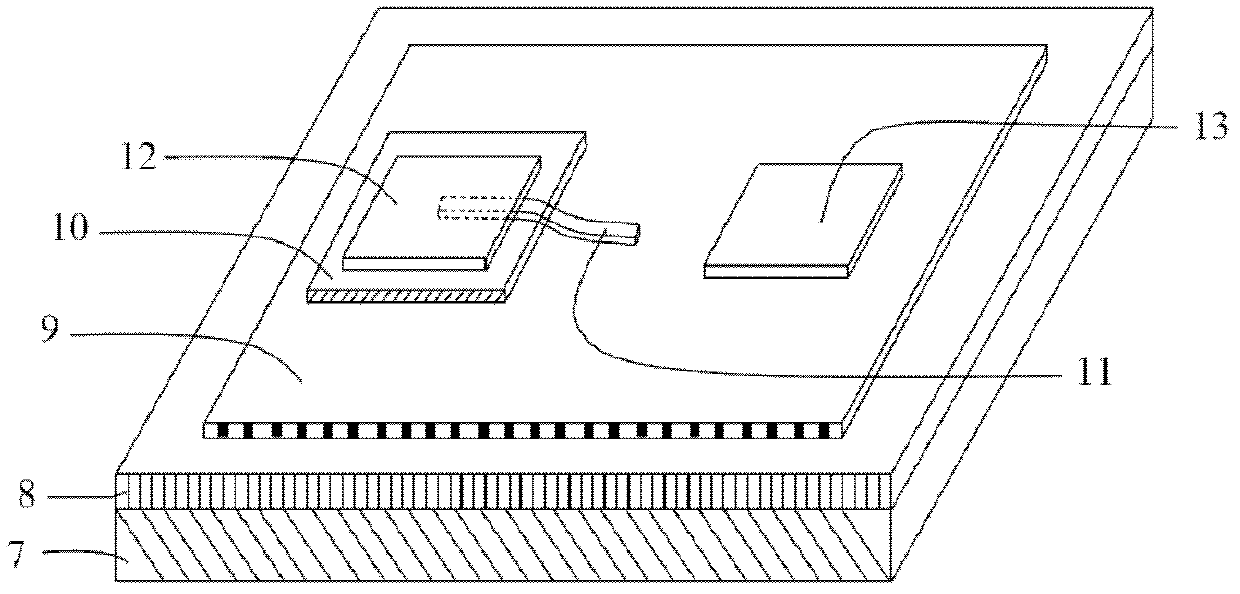
[0042] Such as figure 2 As shown, the P-type zinc telluride nanoribbon and N-type graphene heterojunction photodetector in this embodiment have the following structure:
[0043] Graphene 9 is tiled on the surface of a silicon substrate 7 covered with a silicon dioxide layer 8, and a 30-nanometer thick insulating layer 10 is arranged on the graphene 9, and zinc telluride nanometers are dispersed on the surface of the insulating layer 10. Belt 11 and a part of the zinc telluride nanobelt 11 is in contact with graphene 9; a 100 nanometer thick gold electrode 12 is provided on the insulating layer 10, and the gold electrode 12 is in ohmic contact with the zinc telluride nanobelt 11; On the graphene 9, a 100 nanometer thick gold electrode 13 is provided, and the gold electrode 13 is isolated from the insulating layer 10, the gold electrode 12 and the zinc telluride nanoribbon 11;
[0044] The zinc telluride nanobelt 11 is a P-type zinc telluride nanobelt; the graphene 9 is an N-t...
PUM
 Abstract
Description
Claims
Application Information
 - R&D
- Intellectual Property
- Life Sciences
- Materials
- Tech Scout
- Unparalleled Data Quality
- Higher Quality Content
- 60% Fewer Hallucinations
Browse by: Latest US Patents, China's latest patents, Technical Efficacy Thesaurus, Application Domain, Technology Topic, Popular Technical Reports.
© 2025 PatSnap. All rights reserved.Legal|Privacy policy|Modern Slavery Act Transparency Statement|Sitemap|About US| Contact US: help@patsnap.com