Array imaging system

An imaging system and array technology, applied in antenna arrays, electrical components, circuits, etc., can solve the problems of high cost, small waveguide size, increased waveguide loss, etc., and achieve the effect of quick and convenient coating

Inactive Publication Date: 2012-07-18
ZIJINSHAN ASTRONOMICAL OBSERVATORY CHINESE ACAD OF SCI
View PDF6 Cites 5 Cited by
  • Summary
  • Abstract
  • Description
  • Claims
  • Application Information

AI Technical Summary

Problems solved by technology

However, as the frequency increases, the size of the waveguide becomes smaller and smaller (closer to the working wavelength), and the processing and production are technically difficult and costly.
In addition, the skin depth of the metal surface decreases with the increase of the frequency, that is to say, the high-frequency current is more and more concentrated on the surface of the waveguide, and the surface roughness of the metal waveguide causes the waveguide loss to increase sharply with the frequency.
At the same time, the waveguide horn and its corresponding connecting waveguide are usually manufactured by machining, which is not suitable for large-scale array applications

Method used


Image

  • Array imaging system
  • Array imaging system
  • Array imaging system

Examples


Embodiment 1

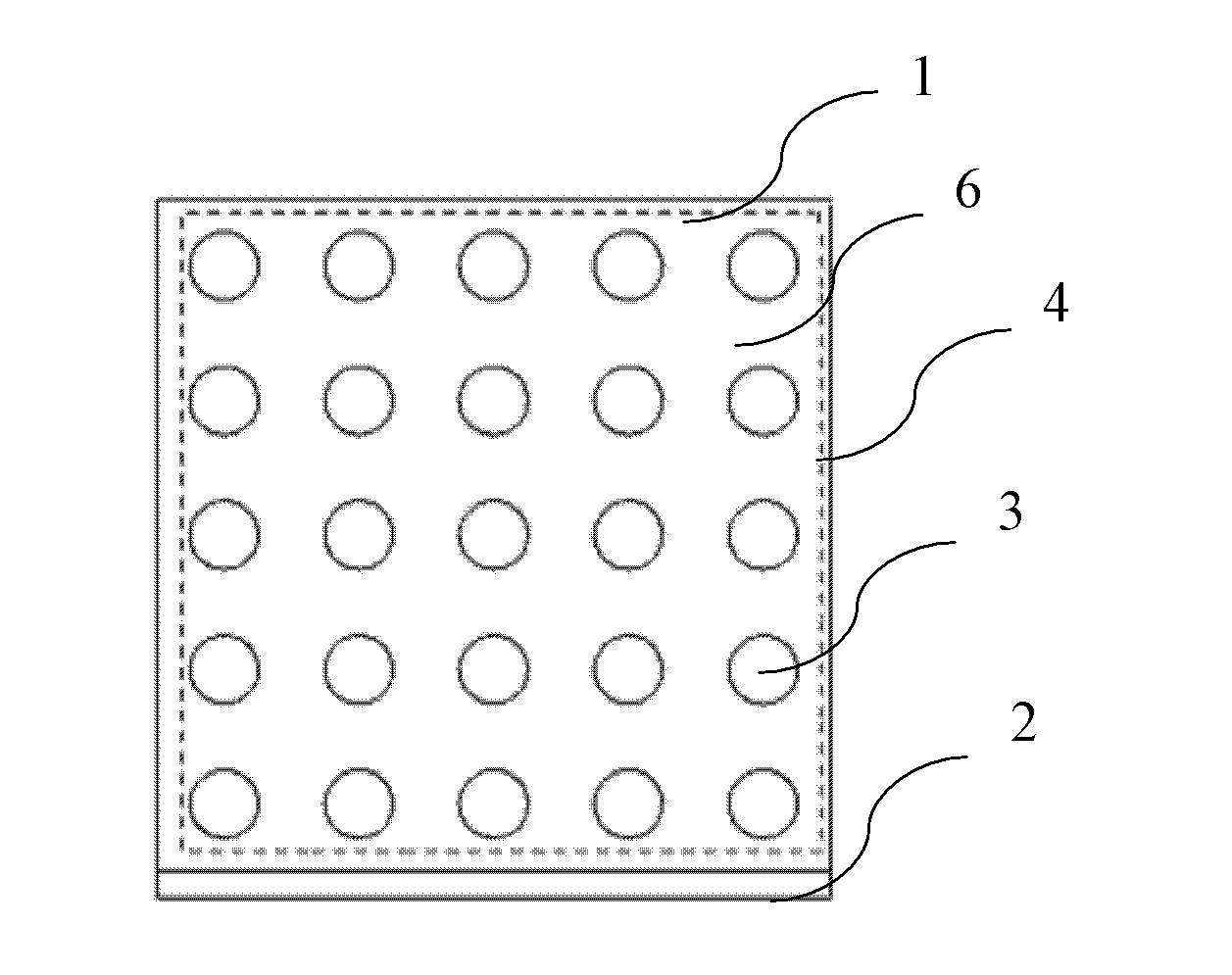
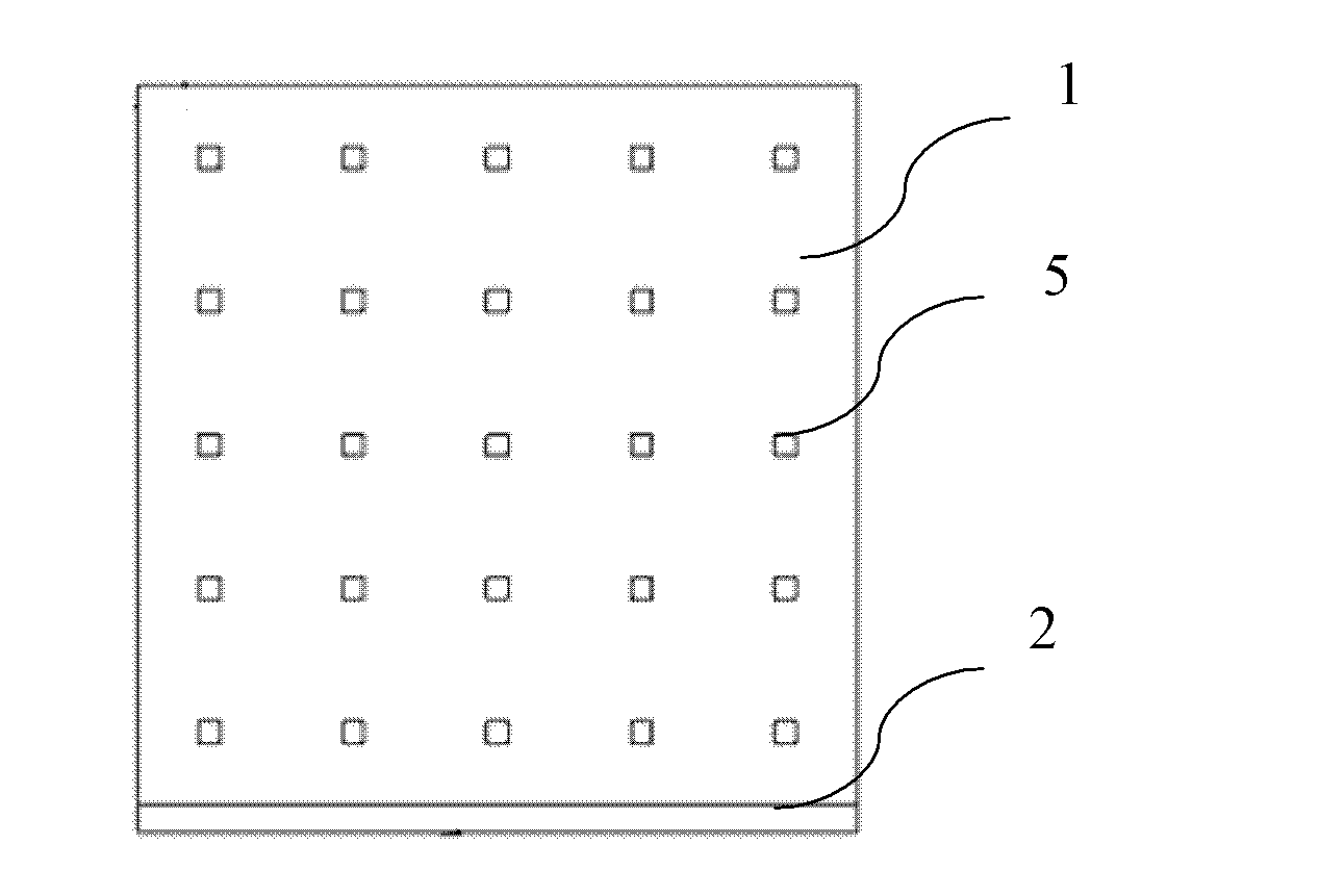
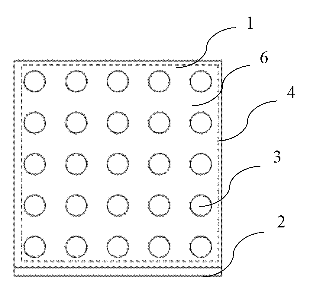
[0018] Embodiment 1, with reference to figure 1 and figure 2 , an array imaging system 1, including a base 2 and a 5×5 silicon lens array 4 composed of 25 silicon lenses 3 arranged on the base 2 ( figure 1 In the dotted line box of ), the front surface of the silicon lens 3 is coated with an anti-reflection layer with a thickness of 1 / 4 wavelength, and a terahertz detector 5 is respectively arranged in the center of the back of each silicon lens 3 to form a terahertz detector For the array, on the front surface of the base 2 , the metal surface between several silicon lenses 3 is covered with a layer 6 of terahertz wave-absorbing material.

[0019] The manufacturing method of the terahertz absorbing material layer 6 is as follows:

[0020] 1) Clean the front surface of the base 2 of the detector array;

[0021] 2) Use a knife or scissors to cut the terahertz absorbing material into the shape of the metal surface of the detector array;

[0022] 3) Use a pressure-sensitive ...

Embodiment 2

[0026] This example is basically the same as Example 1, but the material used for the terahertz wave-absorbing material layer 6 is a terahertz radiation-absorbing surface layer made of Stycast and SiC, and the surface layer includes a black first Stycast epoxy resin layer. A SiC particle layer is provided on the first Stycast epoxy resin layer, and a second Stycast epoxy resin layer is provided on the SiC particle layer. That is, the first and second Stycast epoxy layers stick the SiC particle layer to the metal surface.

[0027] The manufacturing method of the terahertz absorbing material layer 6 is as follows:

[0028] 1) Clean the metal surface of the base and roughen the surface with sandpaper;

[0029] 2) First layer of Stycast epoxy on the surface painted black;

[0030] 3) Sprinkle a layer of SiC particles on the surface, with a diameter of about 0.1 mm;

[0031] 4) Finally, apply a second layer of black Stycast epoxy resin to fix the SiC particles;

[0032] 5) Wait...


PUM


Abstract

The invention relates to an array imaging system. The system comprises a base and a silicon lens array which is arranged on the base and formed by a plurality of silicon lenses, an anti-reflect layer with thickness of a quarter of a wavelength is plated on the surface of the frontal side of each of the silicon lens, a terahertz probe is installed in the center of the back of each of the silicon lens to form a terahertz probe array, and a terahertz wave-absorbing material layer is covered on a metal surface among the plurality of the silicon lenses on the frontal side of the base.

Description

technical field [0001] The invention relates to a radio astronomical telescope, in particular to an array imaging system. Background technique [0002] Terahertz superconducting detectors are high-sensitivity detectors widely used in radio astronomy receivers. In order to achieve efficient signal coupling with the main antenna of a radio astronomy telescope, it is particularly important to accurately characterize the far-field beam characteristics of superconducting detectors. When the frequency is lower than 1.5 THz, the waveguide superconducting detector integrates the waveguide horn as the receiving antenna, which has good beam characteristics. However, as the frequency increases, the size of the waveguide becomes smaller and smaller (closer to the working wavelength), and the processing and fabrication are technically difficult and costly. In addition, the skin depth of the metal surface decreases as the frequency increases, that is to say, the high-frequency current i...

Claims


Application Information

Patent Timeline
Patent Type & Authority Applications(China)
IPC IPC(8): H01Q17/00H01Q19/06H01Q21/00
Inventor 张文缪巍史生才
Owner ZIJINSHAN ASTRONOMICAL OBSERVATORY CHINESE ACAD OF SCI
Why Eureka
Try Eureka