Electrophotographic photoconductor and image forming apparatus including the same
A technology of photoconductor and electrophotography, which is applied to the equipment of the electric recording process using the charge pattern, the electric recording process using the charge pattern, optics, etc., and can solve the problem of insufficient gas resistance effect, deterioration of the electrical characteristics of the photoconductor, and the like. Improve environmental stability, improve image forming speed, and ozone resistance environmental stability by solving problems such as degradation of electrophotographic characteristics
- Summary
- Abstract
- Description
- Claims
- Application Information
AI Technical Summary
Problems solved by technology
Method used
Image
Examples
Embodiment approach
[0134] Hereinafter, embodiments of the electrophotographic photoconductor and image forming apparatus of the present invention will be described with reference to the drawings.
[0135] However, the electrophotographic photoconductor and image forming apparatus of the present invention are not limited to the following embodiments, and it will be clear to those skilled in the art from the description herein and the accompanying drawings that the present invention includes Various modifications, changes and alterations may be made to any of the embodiments within the given range.
[0136] Multilayer Electrophotographic Photoconductor
Embodiment approach 1
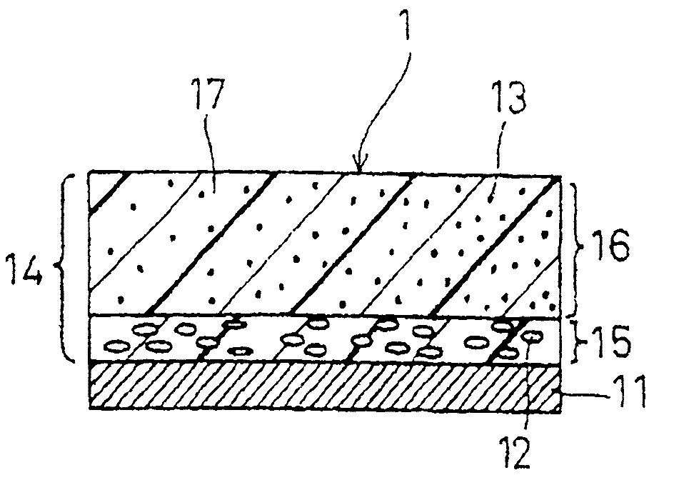
[0138] figure 1 is a partial cross-sectional plan view schematically showing the configuration of an electrophotographic photoconductor 1 that is Embodiment Mode 1 of the electrophotographic photoconductor of the present invention. In this embodiment mode, the photosensitive layer has a multilayer structure including a charge generating layer and a charge transporting layer.
[0139] The electrophotographic photoconductor 1 includes: a sheet-shaped conductive carrier 11 formed of a conductive material; a charge generating layer 15 stacked on the conductive carrier 11 and including a charge generating material 12; and a charge generating layer 15 stacked on the charge generating layer 15 and including a charge transport Charge transport layer 16 of material 13 . The charge generation layer 15 and the charge transport layer 16 constitute a multilayer type photoconductive layer 14 as a photosensitive layer. In other words, the photoconductor 1 is a multilayer type photoconducto...
Embodiment approach 2
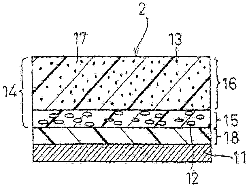
[0223] figure 2 is a partial cross-sectional plan view schematically showing the configuration of an electrophotographic photoconductor 2 which is Embodiment Mode 2 of the electrophotographic photoconductor of the present invention. The electrophotographic photoconductor 2 of the present embodiment and figure 1 The electrophotographic photoconductor 1 of Embodiment Mode 1 shown in .
[0224] middle layer
[0225] It should be noted that the electrophotographic photoconductor 2 has the intermediate layer 18 between the conductive support 11 and the photosensitive layer 14 .
[0226] When the intermediate layer 18 is not provided between the conductive carrier 11 and the photosensitive layer 14, charges will be injected from the conductive carrier 11 into the photosensitive layer 14, thereby reducing the chargeability of the photosensitive layer 14, thereby causing the The surface charge decreases and produces image defects including image fogging. In forming an image by th...
PUM
 Abstract
Description
Claims
Application Information
 - Generate Ideas
- Intellectual Property
- Life Sciences
- Materials
- Tech Scout
- Unparalleled Data Quality
- Higher Quality Content
- 60% Fewer Hallucinations
Browse by: Latest US Patents, China's latest patents, Technical Efficacy Thesaurus, Application Domain, Technology Topic, Popular Technical Reports.
© 2025 PatSnap. All rights reserved.Legal|Privacy policy|Modern Slavery Act Transparency Statement|Sitemap|About US| Contact US: help@patsnap.com


