Eureka AIR delivers breakthrough ideas for toughest innovation challenges, trusted by R&D personnel around the world.

Production method of stepped groove circuit board with through hole, soldermask and circuit graphics at groove bottom

A technology of circuit graphics and manufacturing methods, which is applied in the direction of multilayer circuit manufacturing, secondary processing of printed circuits, and electrical connection formation of printed components, etc. It can solve the problems of bubbling, failure to manufacture, and cracking of laminated prepregs to prevent peeling Effect

Active Publication Date: 2012-07-04
DONGGUAN SHENGYI ELECTRONICS
View PDF2 Cites 37 Cited by
  • Summary
  • Abstract
  • Description
  • Claims
  • Application Information

AI Technical Summary

Problems solved by technology

And for the through hole at the bottom of the groove that cannot be plugged (such as a plug hole), it cannot be made
At the same time, there is a problem that the solder mask at the bottom of the groove is easy to peel off during lamination under high temperature and pressure
In addition, the embedded gaskets in the traditional production method often use silica gel sheets. Due to the gaps inside the silica gel sheets, the residual water vapor expands under high temperature and high pressure, resulting in bubbling and cracking of the laminated prepreg.

Method used


Image

  • Production method of stepped groove circuit board with through hole, soldermask and circuit graphics at groove bottom
  • Production method of stepped groove circuit board with through hole, soldermask and circuit graphics at groove bottom
  • Production method of stepped groove circuit board with through hole, soldermask and circuit graphics at groove bottom

Examples


Embodiment Construction

[0021] like Figure 1 to Figure 8 Shown, the manufacturing method of the stepped groove circuit board of groove bottom tool through hole, solder resist and circuit pattern of the present invention, comprises the following steps:

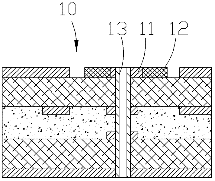
[0022] Step 1: make the sub-board 10, the sub-board 10 is facing the step groove 80 to be made ( Figure 8 As shown), one side of the circuit pattern 11 and solder resist 12 are made, and the position of the prepared sub-board and the step groove 80 to be made is made with a metallized through hole 13, such as figure 2 Shown is a schematic structural view of the fabricated sub-board 10;

[0023] Step 2: Provide a prepreg 20 and a core board 30 (core boards of other layers except the sub-board 10 ) on which the circuit pattern has been made, and open a through groove 21 on the prepreg 20 adjacent to the sub-board 10 ;

[0024] Step 3: laminate the sub-board 10, the prepreg 20 and the core board 30 according to a predetermined stacking sequence, and...


PUM


Abstract

The invention relates to a production method of a stepped groove circuit board with a through hole, a soldermask and a circuit graphics at a groove bottom, which comprises the following steps that: 1, a sub board is produced, and is provided with the circuit graphics, the soldermask and the metalized through hole; 2, a prepreg and a core board are provided, and a through groove is arranged at the prepreg; 3, packing is carried out, a polytetrafluoroethylene (PTFE) gasket is placed in the through groove, and a polyimide adhesive tape is adhered to one side of the PTFE gasket, which is close to the sub board; 4, lamination is carried out, so a mother board is produced; 5, the through hole is drilled on the mother board, a protective adhesive tape is adhered to the outer end of the metalized through hole, and then copper deposition and electroplating are carried out; 6, the protective adhesive tape is removed, and an outer layer of circuit graphics is produced; 7, the outer layer is subjected to soldermask treatment, the board is milled in a depth control way, and a stepped groove is formed; and 8, the PTFE gasket and the polyimide adhesive tape are taken out, surface treatment is carried out, so the stepped groove circuit board is produced. According to the production method, the stepped groove circuit board of which the through hole at the groove bottom cannot be blocked can be produced, and the soldermask of the groove bottom is good.

Description

technical field [0001] The invention relates to the field of circuit board production, in particular to a method for producing a stepped groove circuit board with through holes at the bottom of the groove, solder resist and circuit patterns. Background technique [0002] For stepped groove circuit boards with circuit patterns, through holes and surface treatment at the bottom of the groove, at present, gaskets are embedded in the groove to resist glue, the circuit pattern and surface treatment of the bottom of the groove are pre-made, and the through holes are plugged. And then can't make for the through hole at the bottom of the groove that can't plug hole (as plug hole). At the same time, there is a problem that the solder resist at the bottom of the groove is easy to peel off during lamination under high temperature and high pressure. In addition, in traditional production methods, silicone sheets are often used for the embedded gaskets. Because there are gaps inside the...

Claims


Application Information

Patent Timeline
Patent Type & Authority Applications(China)
IPC IPC(8): H05K3/46H05K3/42H05K3/28
Inventor 焦其正唐海波辜义成曾志军
Owner DONGGUAN SHENGYI ELECTRONICS
Why Eureka
Eureka Blog
Learn More