High-transmittance low-reflection electromagnetic screening structure for liquid crystal display screen and manufacturing method for structure

An electromagnetic shielding structure, liquid crystal display technology, applied in the fields of magnetic field/electric field shielding, electrical components, optics, etc., can solve the problems of high reflectivity of the transparent conductive shielding layer, affecting the display effect, etc. Readability, the effect of reducing distractions

Inactive Publication Date: 2012-07-04
NO 55 INST CHINA ELECTRONIC SCI & TECHNOLOGYGROUP CO LTD
View PDF3 Cites 7 Cited by
  • Summary
  • Abstract
  • Description
  • Claims
  • Application Information

AI Technical Summary

Problems solved by technology

[0005] The purpose of the present invention is to solve the problem that the existing liquid crystal display metal grid electromagnetic shielding layer is easy to produce interference fringes, and the transparent conductive shielding layer has a large reflectivity, which affects the display effect. High transmission and low reflection electromagnetic shielding structure of liquid crystal display with guaranteed transmittance and manufacturing method thereof

Method used


Image

  • High-transmittance low-reflection electromagnetic screening structure for liquid crystal display screen and manufacturing method for structure
  • High-transmittance low-reflection electromagnetic screening structure for liquid crystal display screen and manufacturing method for structure
  • High-transmittance low-reflection electromagnetic screening structure for liquid crystal display screen and manufacturing method for structure

Examples


Embodiment 2

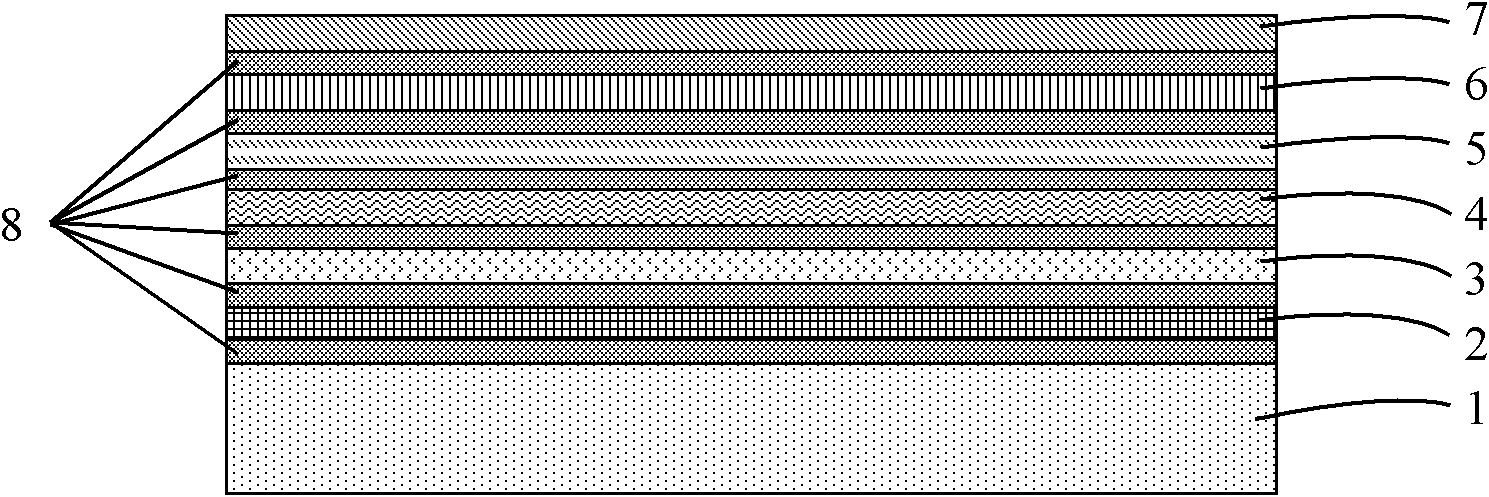
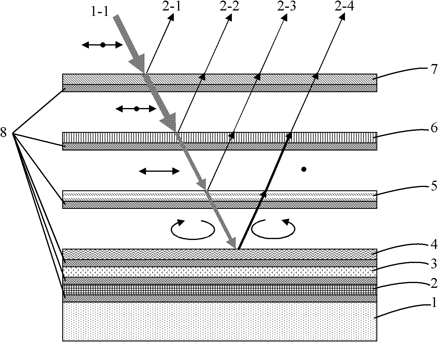
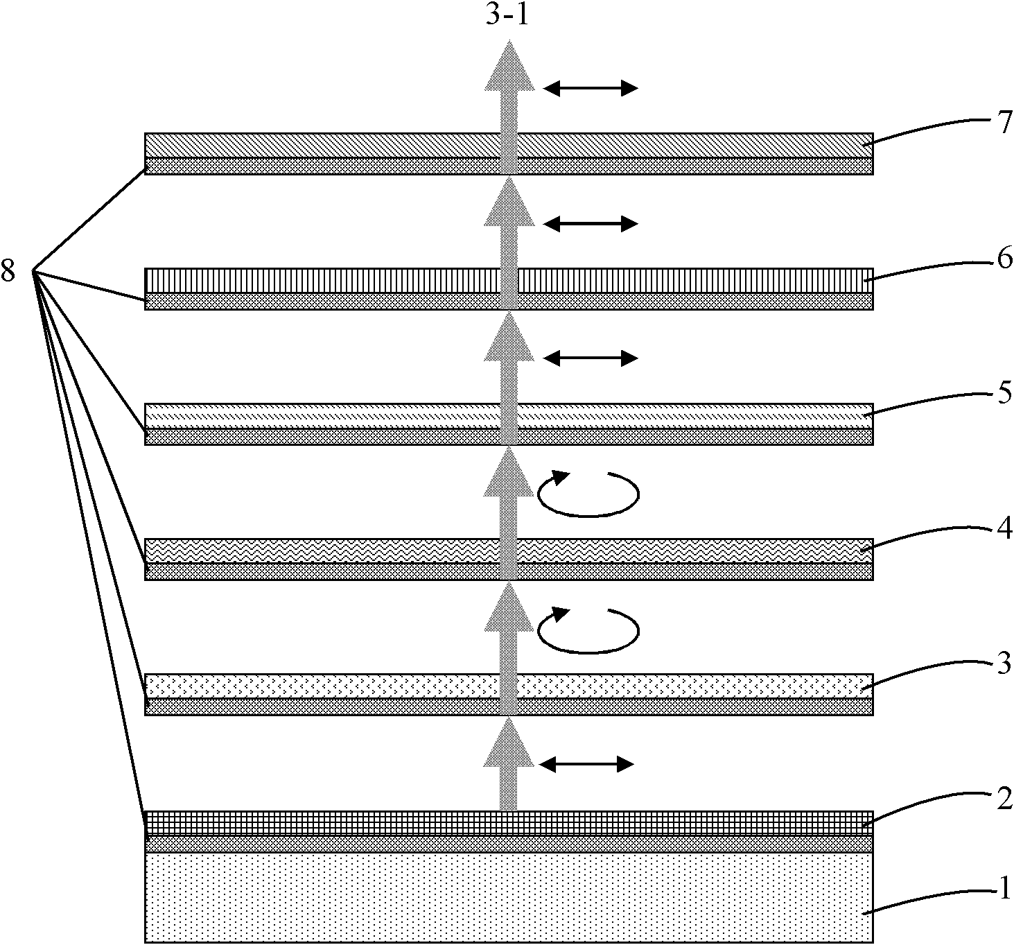
[0036] Such as Figure 4 shown.

[0037] A method for manufacturing an electromagnetic shielding structure with high transmission and low reflection for a liquid crystal display, comprising the following steps: (1) optically bonding the anti-reflection layer 7 and the polarizing layer 6 through a transparent optical adhesive 8 (such as rolling bonding, Liquid glue bonding, etc., the same below) The binding process is solidified into a double-layer structure. (2) The double-layer structure and the quarter-wave retardation layer 5 are cured into a three-layer structure through the transparent optical adhesive 8 by optical bonding and binding process. (3) The three-layer structure and the indium tin oxide transparent conductive layer 4 are cured into a four-layer structure through the transparent optical adhesive 8 by an optical bonding process. (4) The four-layer structure and the quarter-wave retardation layer 3 are cured through the transparent optical adhesive 8 by an optic...


PUM


Abstract

The invention discloses a high-transmittance low-reflection electromagnetic screening structure for a liquid crystal display screen and a manufacturing method for the structure. The structure is characterized by sequentially consisting of a first polarizer layer (2), a first quarter wavelength delaying layer (3), a transparent indium tin oxide conductive layer (4), a second quarter wavelength delaying layer (5), a second polarizer layer (6) and a reflection reducing layer (7) which serve as optical functional layers, wherein the optical functional layers are connected with one another to form a whole body by using transparent optical cement (8) by a binding process; and the first polarizer layer (2) is closely adjacent to the liquid crystal display screen (1). The manufacturing method comprises the following steps of: optically binding the optical functional layers in sequence by using the optical cement and solidifying for shaping. The structure has the advantages of high transmittance and relatively low electromagnetic reflectivity, the advantages of the conventional electromagnetic screening technology and a good effect, and is low in cost.

Description

technical field [0001] The invention relates to a liquid crystal display technology, in particular to an electromagnetic shielding technology of a liquid crystal display, in particular to a high transmission and low reflection electromagnetic shielding structure of a liquid crystal display and a manufacturing method thereof. Background technique [0002] As we all know, display devices such as liquid crystal displays have electromagnetic radiation and electromagnetic interference problems. At present, both in the field of civilian products and in industrial products, the problem of anti-electromagnetic radiation and anti-electromagnetic interference has been raised. Therefore, the electromagnetic shielding technology in the display window area of ​​​​display devices has become a display One of the important technologies for electromagnetic shielding of devices. At present, two technologies are mainly used for electromagnetic shielding in the window area of ​​display devices...

Claims


Application Information

Patent Timeline
IPC IPC(8): G02F1/1335H05K9/00B32B9/04
Inventor 洪乙又余雷王绪丰樊卫华铁斌杨芳郑赛杨洪宝吴添德张小芸吴金华
Owner NO 55 INST CHINA ELECTRONIC SCI & TECHNOLOGYGROUP CO LTD
Why Eureka
Try Eureka