Parallel write-in multi-FIFO (first in,first out) implementation method based on single chip block RAM (random access memory)

An implementation method, a single-chip technology, applied in the field of information technology applications, can solve problems such as low resource utilization, insufficient number of memories, waste, etc., to achieve full utilization, enhance market competitiveness, and improve utilization.

Inactive Publication Date: 2012-06-27
FUSHUN OPTOELECTRONICS TECH
View PDF4 Cites 10 Cited by
  • Summary
  • Abstract
  • Description
  • Claims
  • Application Information

AI Technical Summary

Problems solved by technology

The capacity of a single-chip block RAM is generally relatively large, such as 9Kbit for altera and 18Kbit for xilinx. In general design reality, FIFO as a data cache often does not need such a large capacity, and after a block RAM instantiates a FIFO, The remaining storage space can no longer be used for other purposes and is wasted, resulting in low resource utilization
Especially when the number of FIFOs is large and the depth of each FIFO is small, but each FIFO is required to be able to write in parallel to a certain extent, the FPGA design often has the problem that the overall storage capacity is sufficient, but the number of memories is seriously insufficient.

Method used


Image

  • Parallel write-in multi-FIFO (first in,first out) implementation method based on single chip block RAM (random access memory)
  • Parallel write-in multi-FIFO (first in,first out) implementation method based on single chip block RAM (random access memory)
  • Parallel write-in multi-FIFO (first in,first out) implementation method based on single chip block RAM (random access memory)

Examples


Embodiment Construction

[0051] The present invention will be further described below with reference to the drawings and embodiments.

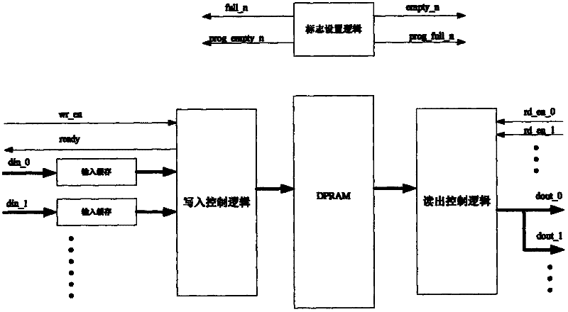
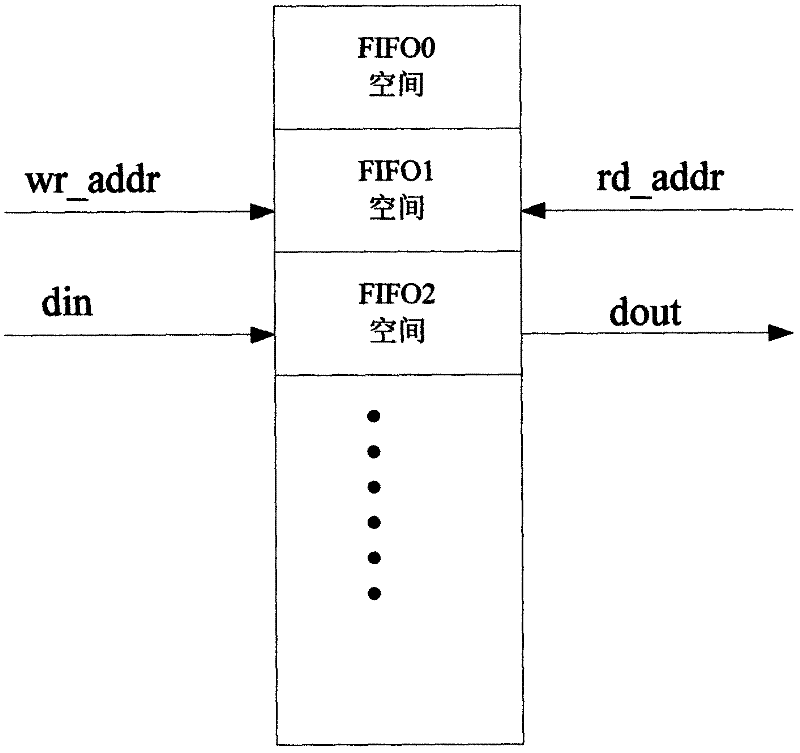
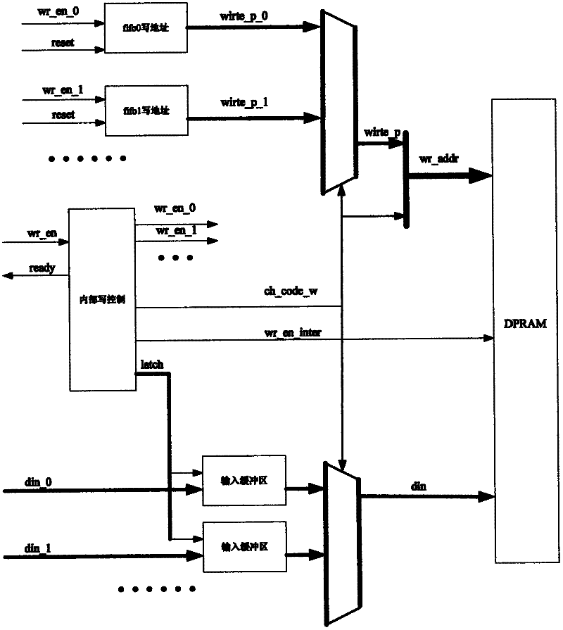
[0052] The present invention proposes a method for realizing multiple FIFOs that require parallel writing and random sequential readout by using a single block RAM. In this method, first use the IP core instantiation tool of the FPGA development platform to instantiate the block RAM into a DPRAM for storing the FIFO data of each channel; the write control logic can accept parallel FIFO data write requirements of each channel, and write the control logic After receiving the external write signal, the data is stored in the corresponding buffer of each channel FIFO, and then the internal write command is generated, and the data of each buffer is written into the storage space corresponding to the DPRAM in turn; when the external read request is received, The read control logic will read the data from the storage space corresponding to the DPRAM according to the requirements...


PUM


Abstract

The invention discloses a parallel write-in multi-FIFO (first in,first out) implementation method based on a single chip block RAM (random access memory). The implementation method comprises the following steps of: instantiating a block RAM into a DPRAM (dual port random access memory) to be used for storing data of each channel FIFO, wherein each channel FIFO has a corresponding memory space in the DPRAM; receiving each channel FIFO parallel data write-in requirement by an input buffer area and a write-in control logic, and writing data to the corresponding input buffer area of each channel FIFO; generating an inner writing order by the input buffer area and the write-in control logic after the input buffer areas receive the data, taking out each channel FIFO data from the input buffer areas; and sequentially writing in the memory space of each channel FIFO; when receiving external any channel FIFO reading requirement, reading the control logic according to the requirement, reading data from the memory space of the channel FIFO, and sending FIFO data to an output port; and setting the marks for marking the empty, full, programmable empty and programmable full states of each channel FIFO for logic. The implementation method provided by the invention can implement a plurality of FIFOs requiring parallel write-in and readout in a random sequence.

Description

Technical field [0001] The invention belongs to the application field of information technology. Specifically, it relates to a method for implementing multiple FIFOs that require parallel writing and random sequential readout by using a single block RAM, and provides a solution for the application of low-cost FPGAs. Background technique [0002] With the development of large-scale programmable technology, the application of FPGA is more and more widely used in electronic design. FPGA is mainly composed of input and output control block, programmable logic block, programmable wiring, embedded memory block (block RAM) and other parts. Among them, block RAM is a very valuable on-chip resource with flexible applications and powerful functions. RAM can be customized to achieve , ROM, CAM, DPRAM, FIFO and other storage structures. Among them, FIFO is particularly widely used, and it is almost indispensable in data buffering and asynchronous clock domain data transmission. For low-en...

Claims


Application Information

Patent Timeline
Patent Type & Authority Applications(China)
IPC IPC(8): G06F5/06
Inventor 邹复民龚志鹏姚进根陈建顺杨伟艺
Owner FUSHUN OPTOELECTRONICS TECH
Why Eureka
Try Eureka