MEMS integration method

A patterned, regional technology, applied in the field of micro-electronic mechanical systems and integrated circuit IC processing technology, MEMS chip manufacturing field containing CMOS circuits, to simplify the integrated manufacturing process, reduce parasitic capacitance and distributed capacitance, and reduce difficulty.

Inactive Publication Date: 2012-06-27
PEKING UNIV
View PDF6 Cites 14 Cited by
  • Summary
  • Abstract
  • Description
  • Claims
  • Application Information

AI Technical Summary

Problems solved by technology

None of these solutions can solve the above problems well at the same time

Method used


Image

  • MEMS integration method
  • MEMS integration method
  • MEMS integration method

Examples


Embodiment Construction

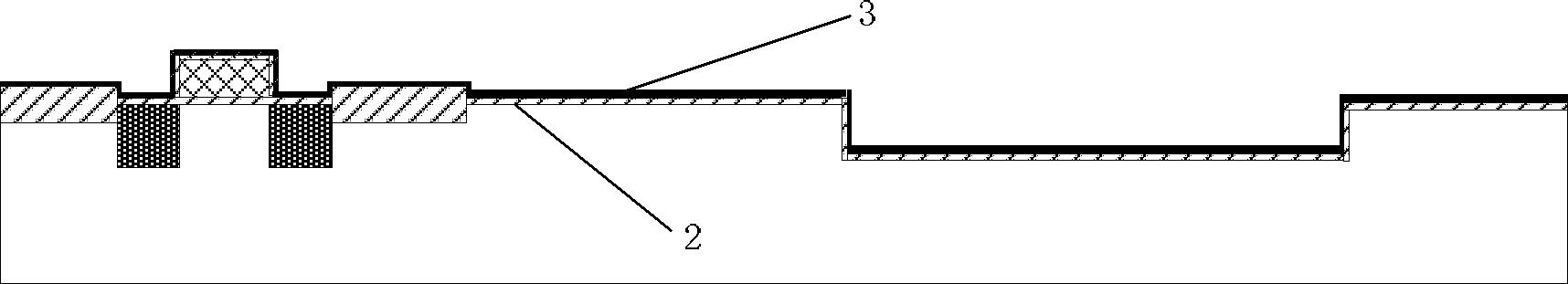
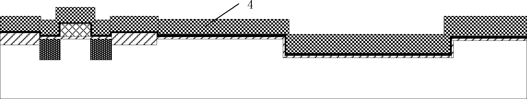
[0038] The MEMS integration method of the present invention is mainly applicable to MEMS device chips made on silicon substrates, including IC parts and movable structures realized by sacrificial layer technology, such as accelerometers, gyroscopes and other sensors, adjustable capacitance structures, etc. device. The following takes the preparation of a monolithic integrated comb-shaped resonator as an example to describe in detail, and the manufacturing steps are as follows:

[0039] 1. A monocrystalline silicon substrate is used as the substrate 1 of the chip, and a concave MEMS region groove 2 is defined and etched by MEMS process photolithography on the substrate 1, as shown in FIG. 1(a);

[0040] 2. Use IC technology to make CMOS circuits outside the MEMS area, complete all processes except metal interconnections, and then deposit IC area protection layers, including: LPCVD silicon oxide LPCVD silicon nitride Form a silicon oxide layer 2 and a silicon nitride layer...


PUM

PropertyMeasurementUnit
Depthaaaaaaaaaa

Abstract

The invention discloses an MEMS integration method. The method comprises steps of: first etching an MEMS area groove, manufacturing a CMOS circuit in an area outside the groove and completing all IC technologies except metal interconnection; then precipitating an IC protective layer and manufacturing an MEMS structure in the groove by employing an MEMS surface sacrificial layer technology; then etching to form lead wire apertures of the IC area, precipitating and imaging the metal to form metal interconnection; finally using photoresist to protect the area outside the groove, removing a sacrificial layer and releasing an MEMS movable structure to obtain a monolithic integration chip. The invention employs MEMS-IC-MEMS intersect manufacturing technology to complete MEMS and IC monolithic integration, reduces height difference between the MEMS structure and the IC through the groove, and reduces pressure of the integration technology on photolithography; meanwhile, technology adjustment avoids metal shedding and improves technology quality and yield.

Description

technical field [0001] The invention belongs to the field of micro-electro-mechanical systems (MEMS) and integrated circuit IC (CMOS) processing technology, and relates to a monolithic integration method of MEMS and IC technology, and adopts a mixed technology method of MEMS-IC-MEMS to simultaneously form MEMS and IC on a single wafer. The CMOS part is especially used in the field of manufacturing MEMS chips containing CMOS circuits. Background technique [0002] There are many advantages of monolithic integration of MEMS and IC, including reducing parasitic capacitance, reducing chip size, reducing cost, reducing packaging pressure, and improving reliability. The difficulties in the integration of MEMS process and IC process mainly include the following points: (1) After the completion of the IC part, the subsequent high-temperature process will affect the distribution of impurities in the active region of the IC, affecting the characteristics of the PN junction and MOS tub...

Claims


Application Information

Patent Timeline
IPC IPC(8): B81C1/00
Inventor 赵丹淇张大成杨芳田大宇刘鹏王玮李婷罗葵
Owner PEKING UNIV
Why Eureka
Try Eureka