Method for preparing tellurium-zinc-cadmium film material with adjustable forbidden bandwidth
A technology of thin film materials and bandgap width, which is applied in the field of preparation of cadmium zinc telluride thin film materials, can solve problems such as difficult to guarantee, difficult to increase Zn element content, difficult to control thin film stoichiometry, etc., to achieve the effect of increasing Zn content
- Summary
- Abstract
- Description
- Claims
- Application Information
AI Technical Summary
Problems solved by technology
Method used
Image
Examples
Embodiment 1
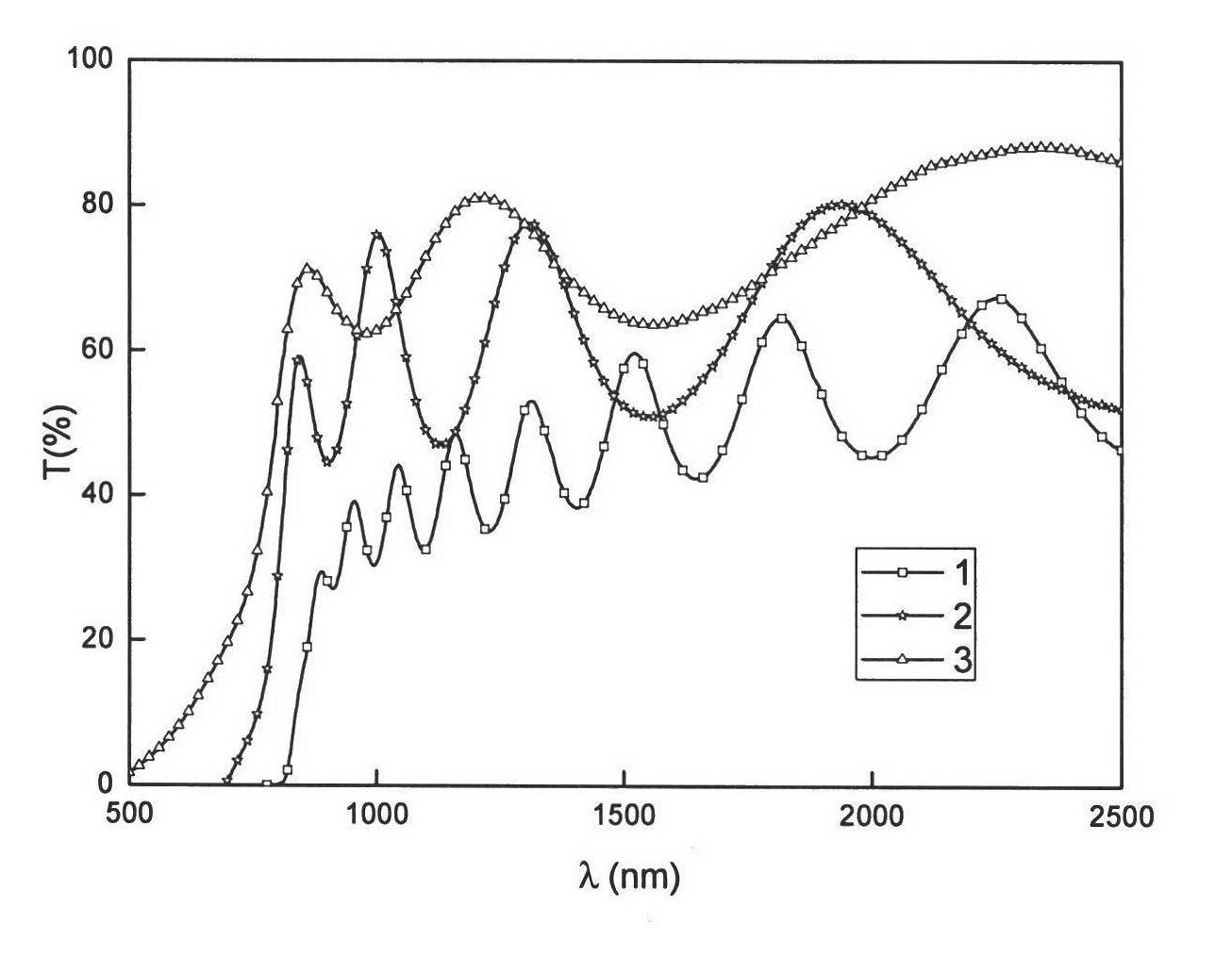
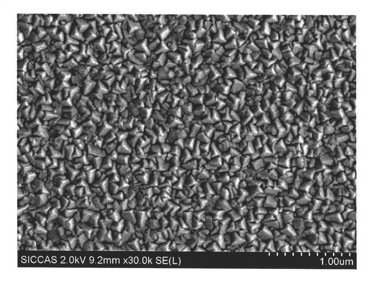
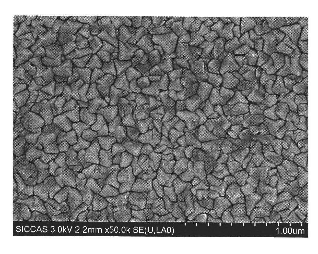
[0022] Clean the glass substrate with an organic solvent such as acetone or alcohol → deionized water → hydrochloric acid → deionized water, and dry it with nitrogen in an ultra-clean environment. Then the glass substrate was fixed on the substrate stage of the magnetron sputtering chamber, and the Cd 0.96 Zn 0.04 The Te target and the Zn target are installed on their respective target guns, and the vacuum of the sputtering chamber is evacuated to 2.9×10 -3 Pa, and then sequentially grow Cd on the glass substrate 0.96 Zn 0.04 Te / Zn / Cd 0.96 Zn 0.04 The thickness of the Te / Zn film is sequentially controlled at 400nm / 50nm / 1000nm / 100nm.
[0023] CD 0.96 Zn 0.04 The magnetron sputtering parameters of the Te film were set as follows: the sputtering power was 36W, the sputtering gas was high-purity Ar gas, the sputtering pressure was 2.4Pa, and the substrate temperature was room temperature.
[0024] The magnetron sputtering parameters of the Zn film were set as follows: the ...
Embodiment 2
[0029] Clean the glass substrate with an organic solvent such as acetone or alcohol → deionized water → hydrochloric acid → deionized water, and dry it with nitrogen in an ultra-clean environment. Then the glass substrate was fixed on the substrate stage of the magnetron sputtering chamber, and the Cd 0.96 Zn 0.04 The Te target and the Zn target are installed on their respective target guns, and the vacuum of the sputtering chamber is evacuated to 2.9×10 -3 Pa, then sequentially grow Zn / Cd on the glass substrate 0.96 Zn 0.04 Te / Zn / Cd 0.96 Zn 0.04 The thickness of the Te / Zn film is sequentially controlled at 10nm / 400nm / 50nm / 1000nm / 100nm.
[0030] Cd 0.96 Zn 0.04 The magnetron sputtering parameters of the Te film were set as follows: the sputtering power was 36W, the sputtering gas was high-purity Ar gas, the sputtering pressure was 2.4Pa, and the substrate temperature was room temperature.
[0031] The magnetron sputtering parameters of the Zn film were set as follows: ...
PUM
 Abstract
Description
Claims
Application Information
 - R&D
- Intellectual Property
- Life Sciences
- Materials
- Tech Scout
- Unparalleled Data Quality
- Higher Quality Content
- 60% Fewer Hallucinations
Browse by: Latest US Patents, China's latest patents, Technical Efficacy Thesaurus, Application Domain, Technology Topic, Popular Technical Reports.
© 2025 PatSnap. All rights reserved.Legal|Privacy policy|Modern Slavery Act Transparency Statement|Sitemap|About US| Contact US: help@patsnap.com


