Semiconductor on insulator and methods of forming same using temperature gradient in an anodic bonding process

An anode connection, semiconductor technology, applied in the fields of semiconductor devices, semiconductor/solid-state device manufacturing, electric solid-state devices, etc., can solve problems such as the limitations of semiconductor materials and insulating substrate characteristics, to simplify equipment, reduce investment and maintenance costs, and increase production. Effect

Inactive Publication Date: 2012-05-30
CORNING INC
View PDF3 Cites 2 Cited by
  • Summary
  • Abstract
  • Description
  • Claims
  • Application Information

AI Technical Summary

Problems solved by technology

[0008] Although the process of manufacturing SOI structure is constantly maturing, the characteristics of the final product made by this process are limited by the characteristics of semiconductor materials and insulating substrates

Method used


Image

  • Semiconductor on insulator and methods of forming same using temperature gradient in an anodic bonding process
  • Semiconductor on insulator and methods of forming same using temperature gradient in an anodic bonding process
  • Semiconductor on insulator and methods of forming same using temperature gradient in an anodic bonding process

Examples


Embodiment Construction

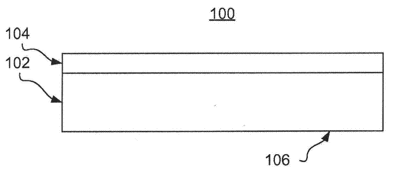
[0025] Referring to the drawings, wherein like reference numerals denote like elements, figure 1 An SOG structure 100 according to one or more embodiments disclosed herein is shown in FIG. The SOG structure 100 may include a glass substrate 102 and a semiconductor layer 104 . The SOG structure 100 has suitable use in the processing of thin film transistors (TFTs), for example, in display applications including organic light emitting diode (OLED) displays and liquid crystal displays (LCD), integrated circuits, photovoltaic devices, and the like.

[0026] The semiconductor material of semiconductor layer 104 may be substantially in the form of a single crystal silicon material. The term "substantially" is used to describe the semiconductor layer 104 in consideration of the fact that semiconductor materials generally contain at least some internal or surface defects, either inherent or intentionally added, e.g., lattice defects or a small amount of grain boundaries. The term ...


PUM


Abstract

Methods and apparatus for producing a semiconductor on glass (SOG) structure include: bringing a first surface of a glass substrate into direct or indirect contact with a semiconductor wafer; heating at least one of the glass substrate and the semiconductor wafer such that a second surface of the glass substrate, opposite to the first surface thereof, is at a lower temperature than the first surface; applying a voltage potential across the glass substrate and the semiconductor wafer; and maintaining the contact, heating and voltage to induce an anodic bond between the semiconductor wafer and the glass substrate via electrolysis.

Description

[0001] Cross-references to related applications [0002] This application claims benefit and priority to U.S. Nonprovisional Patent Application No. 12 / 547,522, filed August 26, 2009, entitled "Semiconductor On Insulator And Methods Of Forming Same Using Temperature Gradient In An Anodic Bonding Process" A semiconductor on and a method of forming the semiconductor using a temperature gradient in an anodic bonding process)", the content of which is relied upon herein and incorporated by reference in its entirety. technical field [0003] The present invention relates to methods of fabricating semiconductor-on-insulator (SOI) structures using an improved anodic bonding process. Background technique [0004] To date, the most widely used semiconductor material in semiconductor-on-insulator structures has been silicon. Such structures are referred to in the literature as silicon-on-insulator structures, and the acronym "SOI" has been applied to such structures. SOI technology ...

Claims


Application Information

Patent Timeline
IPC IPC(8): H01L21/762
CPCH01L21/76251H01L21/76254H01L21/84H01L27/12
Inventor J·G·库亚德
Owner CORNING INC
Why Eureka
Try Eureka