Crystalline silicon solar battery and amorphous silicon solar battery
A technology of solar cells and crystalline silicon cells, which is applied in the field of solar cells to achieve the effects of increased utilization, increased power generation, and improved conversion efficiency
- Summary
- Abstract
- Description
- Claims
- Application Information
AI Technical Summary
Problems solved by technology
Method used
Image
Examples
Embodiment 1
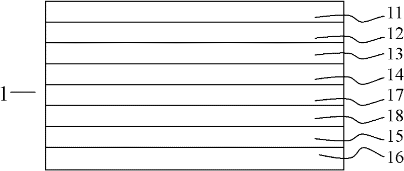
[0026] The structure of the crystalline silicon solar cell of the present embodiment is as figure 1 As shown, it includes an anti-reflection film layer 11 , an ultra-clear rolled glass layer 12 , a second sealing layer 13 , a crystalline silicon cell 14 , a first sealing layer 15 and a TPT backplane 16 combined in sequence. There is also 0.5wt% CeO in the ultra-clear rolled glass layer 12 2 and 1 wt% of Sm 2 o 3 Emitters of rare earth oxides. Among them, the thickness of the antireflection film layer 11 is 100nm, and the material is silicon dioxide; the thickness of the ultra-clear rolled glass layer 12 is 3.2mm; the thickness of the second sealing layer 13 is 0.38mm, and the material is EVA; the thickness of the first sealing layer 15 is It is 0.38mm and the material is EVA.
[0027] The crystalline silicon solar cell of this embodiment 1 utilizes Ce and Sm ions to absorb ultraviolet light and down-convert and emit visible light, so that the ultraviolet light originally a...
Embodiment 2
[0029] The structure of the crystalline silicon solar cell of the present embodiment is as figure 1 As shown, it includes an anti-reflection film layer 11 , an ultra-clear rolled glass layer 12 , a second sealing layer 13 , a crystalline silicon cell 14 , a first sealing layer 15 and a TPT backplane 16 combined in sequence. In the second sealing layer 13 , the organic luminescent dye Lumogen-F 570 is doped with a luminous body, accounting for 2% of the volume of the second sealing layer 13 . Among them, the thickness of the antireflection film layer 11 is 100nm, and the material is silicon dioxide; the thickness of the ultra-clear rolled glass layer 12 is 3.2mm; the thickness of the second sealing layer 13 is 0.38mm, and the material is EVA; the thickness of the first sealing layer 15 is It is 0.38mm and the material is EVA.
[0030] The second sealing layer 13 of the crystalline silicon solar cell in Example 2 is doped with organic luminescent dye Lumogen-F 570, which absorb...
Embodiment 3
[0032] The structure of the crystalline silicon solar cell of the present embodiment is as figure 2 As shown, it includes an anti-reflection film layer 11, an ultra-clear rolled glass layer 12, a second sealing layer 13, a double-sided crystalline silicon cell sheet 14, an up-conversion luminescent film layer 17, a specular reflection layer 18, and a first sealing layer combined in sequence. connection layer 15 and TPT backplane 16. Doping 1% of rare earth Eu ion luminescent material in the anti-reflection film layer 11 . Wherein, the thickness of the anti-reflection film layer 21 is 100nm, and the material is a silicon dioxide film; the up-conversion light-emitting film layer 17 is NaYF doped with 1% Er and 1% Yb rare earth oxide. 4 The thickness of the up-conversion luminescent film layer 17 is 100nm; the thickness of the specular reflection layer 18 is 20nm, and the material is aluminum film; other materials are the same as above.
[0033] In the double-sided crystalline...
PUM
| Property | Measurement | Unit |
|---|---|---|
| Thickness | aaaaa | aaaaa |
| Thickness | aaaaa | aaaaa |
| Thickness | aaaaa | aaaaa |
Abstract
Description
Claims
Application Information
 - R&D
- Intellectual Property
- Life Sciences
- Materials
- Tech Scout
- Unparalleled Data Quality
- Higher Quality Content
- 60% Fewer Hallucinations
Browse by: Latest US Patents, China's latest patents, Technical Efficacy Thesaurus, Application Domain, Technology Topic, Popular Technical Reports.
© 2025 PatSnap. All rights reserved.Legal|Privacy policy|Modern Slavery Act Transparency Statement|Sitemap|About US| Contact US: help@patsnap.com


