Preparation method of antifouling material having crossed regular microstructure on surface
A microstructure and cross-shaped technology, which is applied in the preparation of anti-fouling materials and the field of anti-fouling materials, can solve problems such as biofouling hazards, achieve good anti-adhesion performance, reduce attachment sites, and reduce the effect of contact area
- Summary
- Abstract
- Description
- Claims
- Application Information
AI Technical Summary
Problems solved by technology
Method used
Image
Examples
Embodiment 1
[0016] Embodiment 1: Preparation of cross-shaped microstructure material
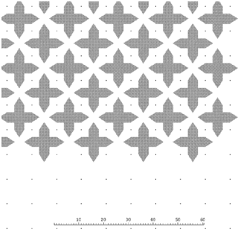
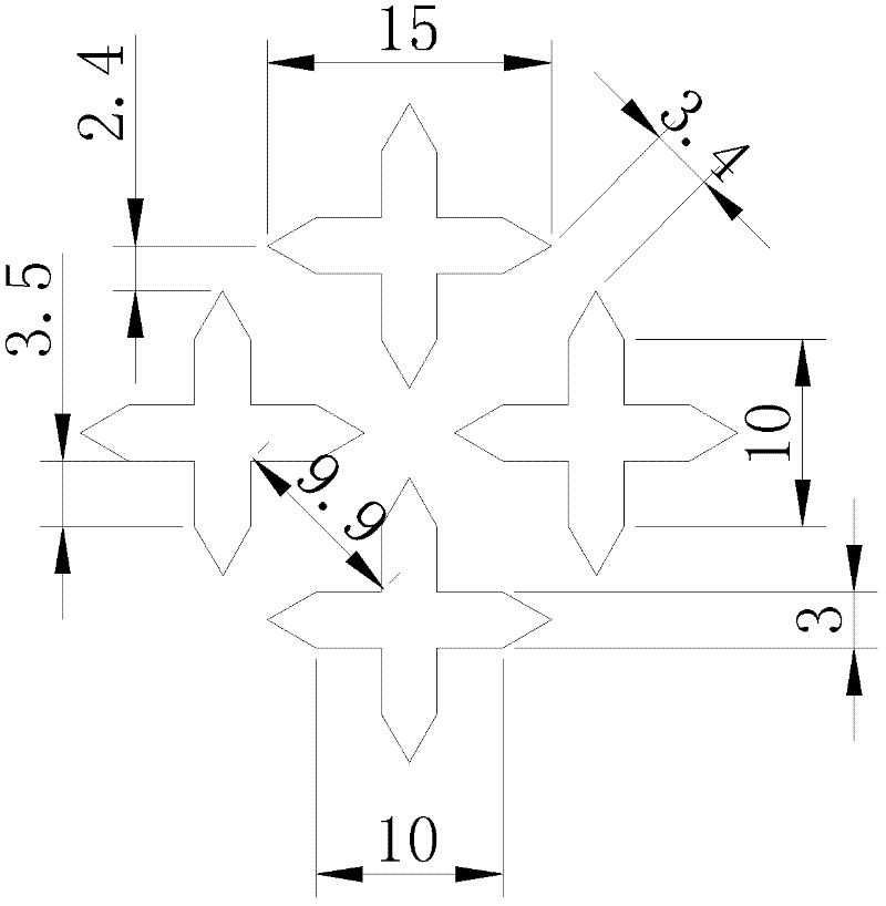
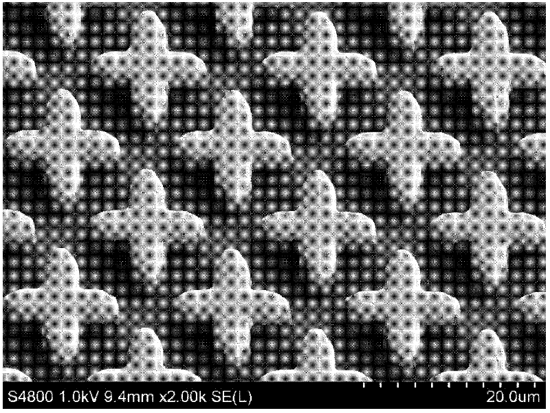
[0017] Prepared by electron beam etching with figure 1 The photomask of the pattern shown, the microstructure arrangement is as follows figure 1 , which is a top view directly above the surface of the material, figure 1 Medium scale bars are in microns. A microstructure with a cross-shaped pattern is etched. The basic units are cross-column-shaped and arranged staggered to form an array. The longest point of the cross is 15 microns, the width of the cross is 3 microns, and the distance between the basic units is 3.4 microns. The specific dimensions are as follows: figure 2 As shown, the unit of the scale in the figure is micron; then the silicon wafer is etched by the deep silicon etching method, etched to a depth of 20 microns in 40 minutes, and a silicon wafer with a depth of 20 microns and a cross-shaped concave pattern can be prepared. Scanning electron microscope photographs of the microstructu...
Embodiment 2
[0020] Prepared by electron beam etching with figure 1 The photomask of the pattern shown, the microstructure arrangement is as follows figure 1 , which is a top view directly above the surface of the material, figure 1 Medium scale bars are in microns. A microstructure with a cross-shaped pattern is etched. The basic units are cross-column-shaped and arranged staggered to form an array. The longest point of the cross is 15 microns, the width of the cross is 3 microns, and the distance between the basic units is 3.4 microns. The specific dimensions are as follows: figure 2 As shown, the unit of the scale in the figure is micron; then the silicon wafer is etched by the deep silicon etching method, and the etching depth is 5 microns in 10 minutes, and a silicon wafer with a depth of 5 microns and a cross-shaped concave pattern can be prepared. Scanning electron microscope photographs of the microstructure image 3 shown.
[0021] Then, take 20g of polydimethylsiloxane and p...
Embodiment 3
[0022] Embodiment 3: the surface contact angle measurement of cruciform microstructure material
[0023] The static contact angles of the polydimethylsiloxane material with a cross-shaped regular microstructure and the polydimethylsiloxane material without microstructure prepared in Example 1 were measured with a static contact angle measuring instrument. It was measured that the static contact angle of the polydimethylsiloxane material without microstructure was 111.9°, and the static contact angle of the polydimethylsiloxane material with cross-shaped microstructure prepared in Example 1 was 140.7°. The existence of the surface microstructure significantly improves the hydrophobicity of the material.
PUM
| Property | Measurement | Unit |
|---|---|---|
| Static contact angle | aaaaa | aaaaa |
Abstract
Description
Claims
Application Information
 - R&D
- Intellectual Property
- Life Sciences
- Materials
- Tech Scout
- Unparalleled Data Quality
- Higher Quality Content
- 60% Fewer Hallucinations
Browse by: Latest US Patents, China's latest patents, Technical Efficacy Thesaurus, Application Domain, Technology Topic, Popular Technical Reports.
© 2025 PatSnap. All rights reserved.Legal|Privacy policy|Modern Slavery Act Transparency Statement|Sitemap|About US| Contact US: help@patsnap.com


