Image shooting device

A technology of camera device and camera unit, which is applied in the direction of image communication, TV, color TV parts, etc., and can solve the problem of damaging the image quality of the camera

Active Publication Date: 2012-03-14
NIKON CORP
View PDF6 Cites 0 Cited by
  • Summary
  • Abstract
  • Description
  • Claims
  • Application Information

AI Technical Summary

Problems solved by technology

[0003] However, in order to shorten the acquisition time of correction data, a method of acquiring correction data only from a part of lines in one screen is adopted. In this case, pixel amplifiers of the lines for which correction data Since pixel amplifiers have different operating points, when used in an area where the input and output characteristics of the pixel amplifier are non-linear, there is a problem that the signal level between lines will vary, which may impair the image quality of the captured image.

Method used


Image

  • Image shooting device
  • Image shooting device
  • Image shooting device

Examples


Embodiment Construction

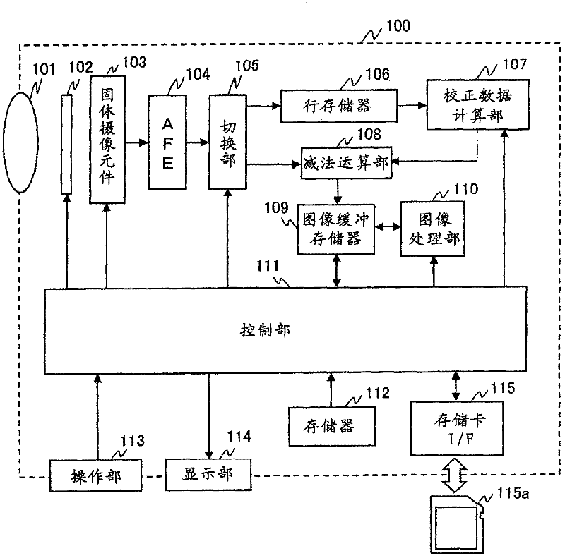
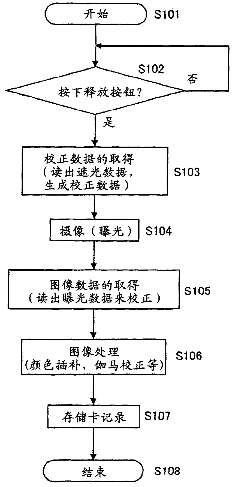
[0023] Hereinafter, embodiments of the imaging device of the present invention will be described in detail using the drawings. figure 1 It is a block diagram showing the structure of the electronic video camera 100 corresponding to the imaging device of the present invention.

[0024] (Structure of electronic camera 100)

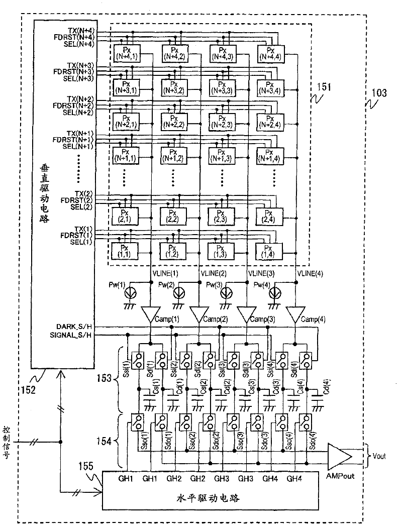
[0025] exist figure 1 Among them, the electronic camera 100 is composed of an optical system 101, a mechanical shutter 102, a solid-state imaging element 103, an AFE (analog front end) 104, a switching unit 105, a line memory 106, a correction data calculation unit 107, a subtraction unit 108, an image buffer memory 109, An image processing unit 110 , a control unit 111 , a memory 112 , an operation unit 113 , a display unit 114 , and a memory card I / F 115 are configured.

[0026] The optical system 101 forms an image of light input from a subject on the light receiving surface of the solid-state imaging device 103 .

[0027] The mechanical shutter 102 is...


PUM


Abstract

An image shooting device includes: an image shooting part formed of a pixel array and a reading control part in which the pixel array includes a plurality of pixels arranged in a matrix form, each of the pixels having a photoelectric conversion part, a transfer transistor, an amplifying transistor, and a reset transistor, and the reading control part performs reading by switching a first reading control in which the reset transistor is controlled to be turned off before exposure to read the pixel signal from a part of rows of the pixel array and a second reading control in which the pixel signal is read from the pixel array after the exposure; and a correcting part correcting the pixel signal read through the second reading control based on the pixel signal read through the first reading control.

Description

technical field [0001] The present invention relates to imaging devices. Background technique [0002] A general electronic camera is equipped with a solid-state imaging element such as a CCD sensor or a CMOS sensor. For example, in the case of a CMOS sensor, charges accumulated by pixels arranged in a matrix on the light receiving surface in response to incident light are converted from charge to voltage by pixel amplifiers and read out to vertical signal lines for each row. And, the signal read from each pixel is read to the outside of the CMOS sensor via a column amplifier, a CDS circuit (correlated double sampling circuit), a horizontal output circuit, and an output amplifier. However, the signal read from the CMOS sensor includes noise components inherent in the row direction, such as fixed pattern noise components and dark shading components. Therefore, in order to remove these noise components, a technique of correcting image data read from the CMOS sensor after exp...

Claims


Application Information

Patent Timeline
Patent Type & Authority Applications(China)
IPC IPC(8): H04N5/225H04N5/235H04N5/357
CPCH04N25/671H04N25/677H04N25/63H04N25/76
Inventor 船水航山中秀记
Owner NIKON CORP
Why Eureka
Try Eureka