


Quick Research
Generate reliable direction feasibility study reports for your R&D in just a few steps.

Technical Q&A
Discover and master advanced knowledge NOW. Basics, ideas, possibilities, all at once.

Find Solutions
As an expert in R&D theories, this can generate solutions to your technical problems instantly.

Evaluate Feasibility
Analyze your overall solution with one click, know your potential R&D risks in advance.

Monitor Landscape
Get weekly tech updates, stay abreast of the latest tech innovations and key insights.
Semiconductor device and method for driving semiconductor device
A driving method and semiconductor technology, applied in the fields of semiconductor devices, semiconductor/solid-state device manufacturing, transistors, etc., can solve the problems of charge injection or removal for a long time, difficult to achieve high-speed writing or erasing, and reduce power consumption. , The effect of ensuring high speed and improving reliability
- Summary
- Abstract
- Description
- Claims
- Application Information
AI Technical Summary
Problems solved by technology
Method used
Image

Examples
Embodiment approach 1
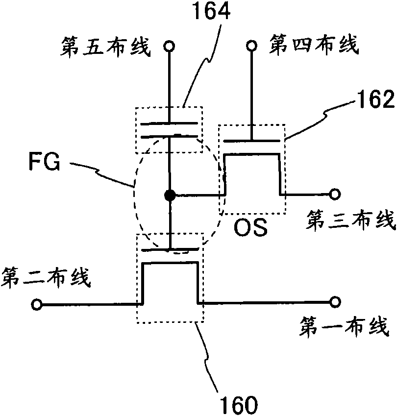
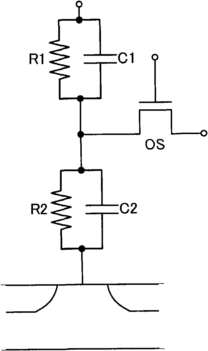
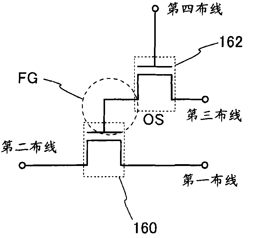
[0058] In this embodiment, refer to Figure 1A-1 , A-2 and 1B and figure 2 The basic circuit configuration and operation of a semiconductor device according to one embodiment of the disclosed invention will be described. In addition, in circuit diagrams, in order to indicate transistors using an oxide semiconductor, the symbol "OS" may be attached.
[0059]
[0060] First, refer to Figure 1A-1 , A-2 and Figure 1B Explain the most basic circuit structure and its operation. exist Figure 1A-1 In the shown semiconductor device, the first line (1st Line) is electrically connected to the source electrode (or drain electrode) of the transistor 160 , and the second line (2nd Line) is electrically connected to the drain electrode (or source electrode) of the transistor 160 . In addition, the third line (3rdLine) is electrically connected to the source electrode (or drain electrode) of the transistor 162 , and the fourth line (4thLine) is electrically connected to the gate elect...
Embodiment approach 2
[0124] In this embodiment, refer to Figure 5A to Figure 10C The structure of a semiconductor device according to one aspect of the disclosed invention and its manufacturing method will be described.
[0125]
[0126] Figure 5A and 5B It is an example of the structure of a semiconductor device. Figure 5A shows a cross-section of a semiconductor device, Figure 5B A plane of a semiconductor device is shown. Figure 5A equivalent to along Figure 5B Sections of A1-A2 and B1-B2. Figure 5A and Figure 5B The shown semiconductor device has a transistor 160 using a first semiconductor material on the lower part and a transistor 162 using a second semiconductor material on the upper part. The first semiconducting material and the second semiconducting material are preferably different materials. For example, a semiconductor material other than an oxide semiconductor may be used as the first semiconductor material, and an oxide semiconductor may be used as the second semico...
Embodiment approach 3
[0261] In this embodiment, use Figures 11A to 11F Now, a case where the semiconductor device described in the above embodiments is applied to electronic equipment will be described. In this embodiment mode, a case where the above-mentioned semiconductor device is used in electronic equipment such as a computer; a mobile phone (also referred to as a mobile phone, a mobile phone device); a portable information terminal (including a portable game machine, an audio playback devices, etc.); video capture devices such as digital cameras and digital video cameras; electronic paper; and television devices (also called television sets or television receivers), etc.
[0262] Figure 11A A notebook personal computer is shown, and includes a housing 701, a housing 702, a display unit 703, a keyboard 704, and the like. The semiconductor device shown in the previous embodiment is provided in at least one of the housing 701 and the housing 702 . Therefore, it is possible to realize a not...
PUM
 Abstract
Description
Claims
Application Information
 - R&D Engineer
- R&D Manager
- IP Professional
- Industry Leading Data Capabilities
- Powerful AI technology
- Patent DNA Extraction
Browse by: Latest US Patents, China's latest patents, Technical Efficacy Thesaurus, Application Domain, Technology Topic, Popular Technical Reports.
© 2024 PatSnap. All rights reserved.Legal|Privacy policy|Modern Slavery Act Transparency Statement|Sitemap|About US| Contact US: help@patsnap.com