Method for manufacturing flash memories

A technology of flash memory and a manufacturing method, which is applied in the manufacture of semiconductor/solid-state devices, electrical components, circuits, etc., can solve the problems of reducing the off-current and increasing the resistance of the device, and achieves the advantages of reducing the off-current, increasing the distance, and increasing the width. Effect

Active Publication Date: 2011-06-01
SHANGHAI HUAHONG GRACE SEMICON MFG CORP
View PDF0 Cites 0 Cited by
  • Summary
  • Abstract
  • Description
  • Claims
  • Application Information

AI Technical Summary

Problems solved by technology

For example, since the thickness of the oxide film on the active region will also be thickened at the same time, the resistance of the source and drain will increase only by thickening the oxide film layer. In the same situation, the cut-off current of the device is reduced

Method used


Image

  • Method for manufacturing flash memories
  • Method for manufacturing flash memories
  • Method for manufacturing flash memories

Examples


Embodiment Construction

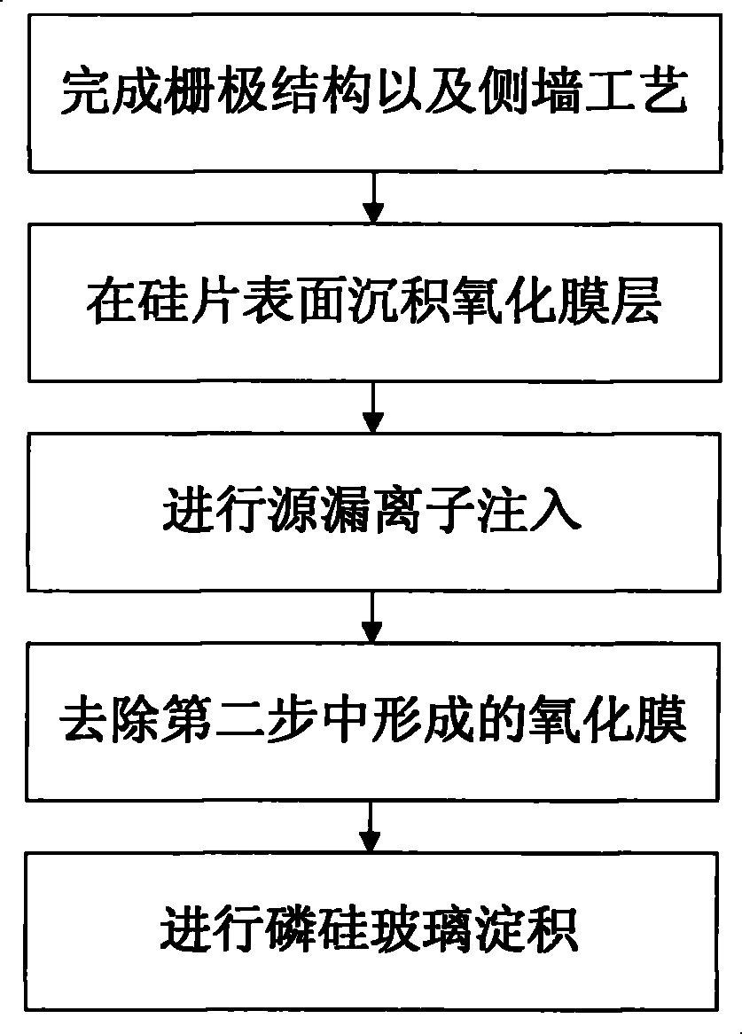
[0030] Such as Figure 9 As shown, the flash memory preparation process of the present invention includes the following steps:,

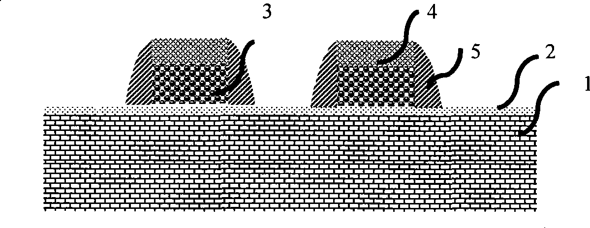
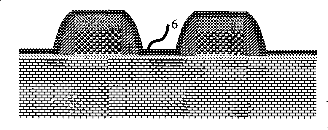
[0031] Firstly, a polysilicon gate is formed using a conventional process and the sidewall is etched. Its structure is as follows: Figure 10 As shown, there is a gate oxide layer 2 on a silicon substrate 1, a polysilicon gate 3 is grown on the gate oxide layer, and a hard mask layer 4 is formed on the polysilicon gate. ) and etching process to form a traditional spacer 5 on the side of the polysilicon gate structure. Then, if Figure 11 As shown, an oxide film 6 is deposited on the surface of the silicon wafer. The oxide film of this layer can increase the distance from the gate to the source and drain, and at the same time play the role of the source and drain injection sacrificial oxide layer.

[0032] Next, if Figure 12 As shown, a layer of nitride film dielectric 9 is deposited. Then, if Figure 13 As shown, the nitride film dielectric ...


PUM


Abstract

The invention discloses a method for manufacturing flash memories. After forming a grid silicon nitride side wall, the method comprises the following steps: 1) depositing a thin oxide film on the surface of a silicon wafer; 2) depositing a nitride film; 3) reversely etching the nitride film deposited in a step 2) and etching the oxide film above a grid structure and in other areas on the surface of the silicon wafer so as to form a flat nitride film side wall; 4) performing source-drain ion implantation; 5) removing the nitride film side wall formed in a step 3); 6) removing the thin oxide film in a step 1) by a wet method; and 7) depositing an interlayer thin film on the surface of the silicon wafer. The method cannot change other characteristics of a device while reducing cut-off current of the device.

Description

technical field [0001] The invention relates to the field of integrated circuit manufacturing technology, in particular to a method for making a flash memory in the field of integrated circuit manufacturing. Background technique [0002] In flash memory devices of 0.13um and below, memory structures with self-aligned contact holes are generally used. In order to reduce the cut-off current of the device without affecting the process window of the subsequent etching of the self-aligned contact hole. The larger the distance between the nitride film sidewalls of the two devices, the larger the process window for subsequent self-aligned contact hole etching. [0003] In order to increase the subsequent self-aligned contact hole etching process window, such as figure 1 As shown, the existing process method for preparing flash memory includes the following process steps: [0004] First, if figure 2 As shown, the gate structure and the side wall process are completed. There is...

Claims


Application Information

Patent Timeline
Patent Type & Authority Patents(China)
IPC IPC(8): H01L21/336H01L21/8247
Inventor 吕煜坤孙娟
Owner SHANGHAI HUAHONG GRACE SEMICON MFG CORP
Why Eureka
Try Eureka