Drive circuit for display device
A technology for driving circuits and display devices, applied in circuits, identification devices, electrical components, etc., can solve problems such as TFT wrong operation, and achieve the effect of preventing wrong operation, preventing the complication of the manufacturing process, and reducing the area.
- Summary
- Abstract
- Description
- Claims
- Application Information
AI Technical Summary
Problems solved by technology
Method used
Image

Examples
no. 1 Embodiment approach
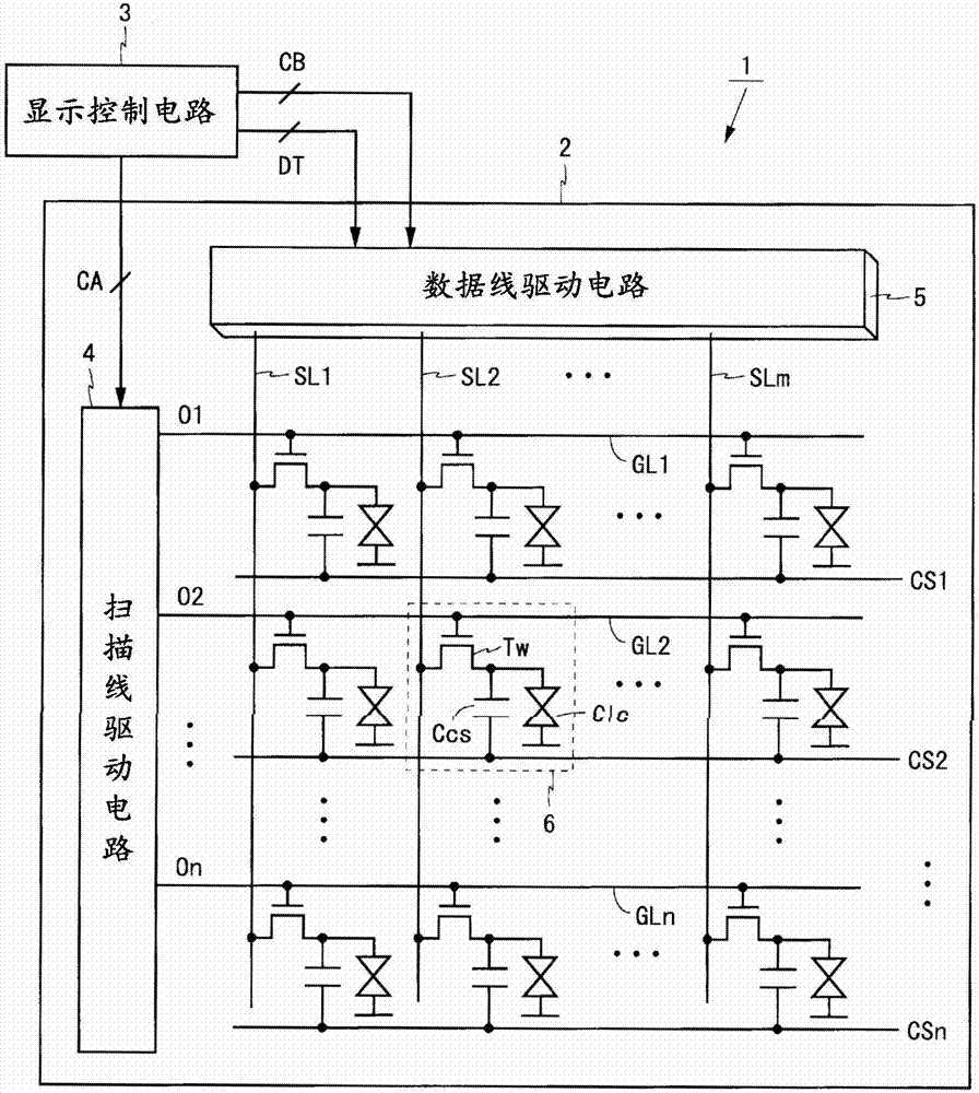
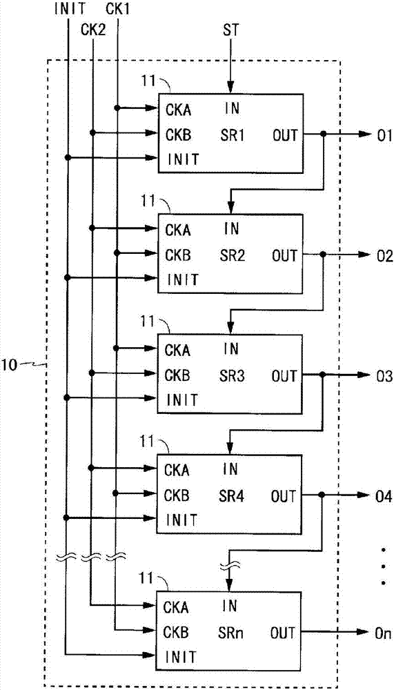
[0067] figure 1 It is a schematic block diagram showing the configuration of a liquid crystal display device including the scanning line drive circuit according to the first embodiment of the present invention. figure 1 The illustrated liquid crystal display device 1 includes a liquid crystal panel 2 , a display control circuit 3 , a scanning line driving circuit 4 and a data line driving circuit 5 .
[0068] The liquid crystal panel 2 includes n scanning lines GL1 -GLn, m data lines SL1 -SLm, n storage capacitor lines CS1 -CSn, and (m×n) pixel circuits 6 . The scanning lines GL1 to GLn are arranged in parallel to each other. The data lines SL1 to SLm are arranged in parallel to each other so as to be perpendicular to the scanning lines GL1 to GLn. The scan lines GL1˜GLn intersect with the data lines SL1˜SLm at (m×n) places. (m×n) pixel circuits 6 are arranged near the intersections of the scanning lines GL1 to GLn and the data lines SL1 to SLm. The storage capacitor lines...
no. 2 Embodiment approach
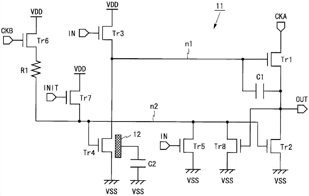
[0105] The scanning line driving circuit according to the second embodiment of the present invention is different from the first embodiment in the method of forming the storage capacitor C2. In this embodiment, the electrode member is formed on the same layer as the channel portion of the transistor to be protected, and is electrically connected to the first conduction electrode of the transistor to be protected. Next, differences between the present embodiment and the first embodiment will be described.
[0106] Figure 9 It is a layout diagram of the transistor Tr4 and its vicinity in the scanning line driving circuit according to the first example of this embodiment. In the first example, in order to form the storage capacitor C2, the electrode member 22 is formed integrally with the semiconductor portion 16 on the semiconductor layer. The semiconductor layer pattern has Figure 10 the shape shown. The expanded portion 20 of the light-shielding film 12 is formed so as t...
no. 3 Embodiment approach
[0111] The scanning line driving circuit according to the third embodiment of the present invention is different from the first and second embodiments in the method of forming the storage capacitor C2. In the present embodiment, the electrode member is electrically connected to one conductive electrode of a transistor other than the transistor to be protected. Next, differences between this embodiment and the first and second embodiments will be described.
[0112] Figure 13 ~ Figure 15 These are layout diagrams of the transistor Tr4 and its vicinity in the scanning line driving circuit according to the first to third examples of this embodiment, respectively. exist Figure 13 ~ Figure 15 Among them, the conduction electrode 31 is the drain or source of other transistors. The blocking potential of the transistor is permanently applied to the conducting electrode 31 . The conduction electrode 31 is electrically connected to a semiconductor portion (not shown) of another tr...
PUM
 Abstract
Description
Claims
Application Information
 - R&D
- Intellectual Property
- Life Sciences
- Materials
- Tech Scout
- Unparalleled Data Quality
- Higher Quality Content
- 60% Fewer Hallucinations
Browse by: Latest US Patents, China's latest patents, Technical Efficacy Thesaurus, Application Domain, Technology Topic, Popular Technical Reports.
© 2025 PatSnap. All rights reserved.Legal|Privacy policy|Modern Slavery Act Transparency Statement|Sitemap|About US| Contact US: help@patsnap.com