Semiconductor device

A semiconductor and device technology, applied in the field of semiconductor devices, can solve problems such as inability to cut off current suppression

Active Publication Date: 2019-02-22
MIE FUJITSU SEMICON
View PDF6 Cites 0 Cited by
  • Summary
  • Abstract
  • Description
  • Claims
  • Application Information

AI Technical Summary

Problems solved by technology

In this case, since the subthreshold leakage current and the junction leakage current vary depending on the concentration of the impurity region, there is a possibility that the off-state current including the sum of these two leakage currents cannot be suppressed low as a result

Method used


Image

  • Semiconductor device
  • Semiconductor device
  • Semiconductor device

Examples


Embodiment Construction

[0040] Some embodiments are described below with reference to the drawings, in which like reference numerals indicate like elements.

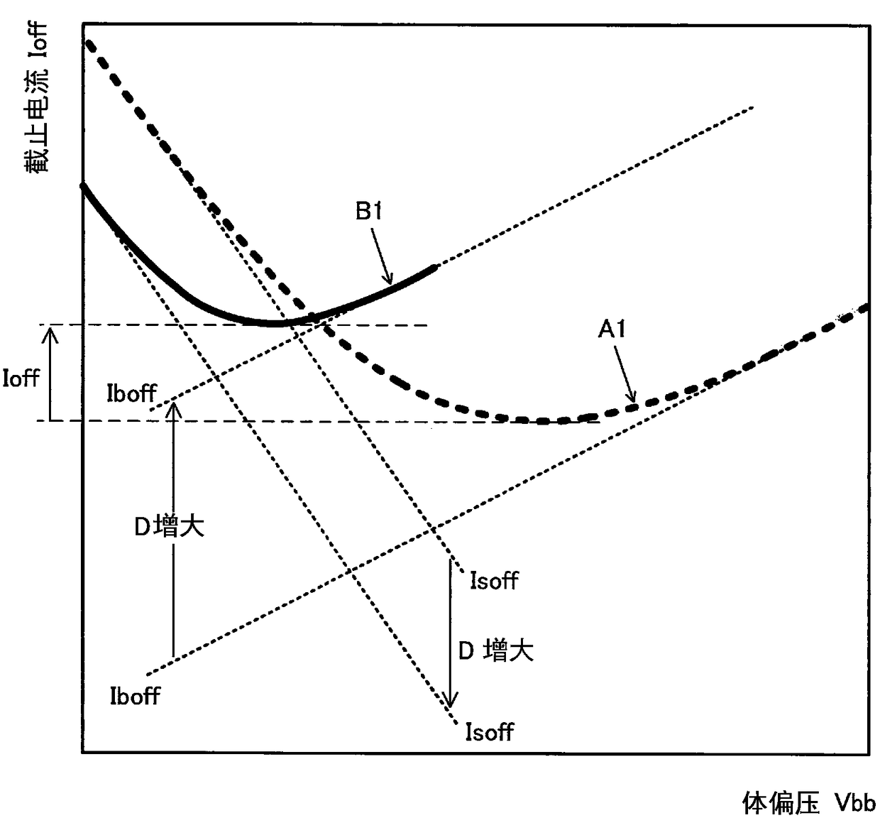
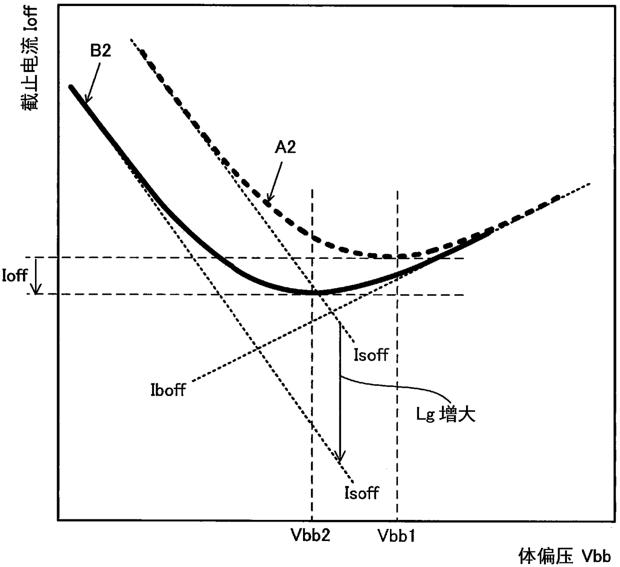
[0041] First, a transistor and its off-state current according to the embodiment will be explained.

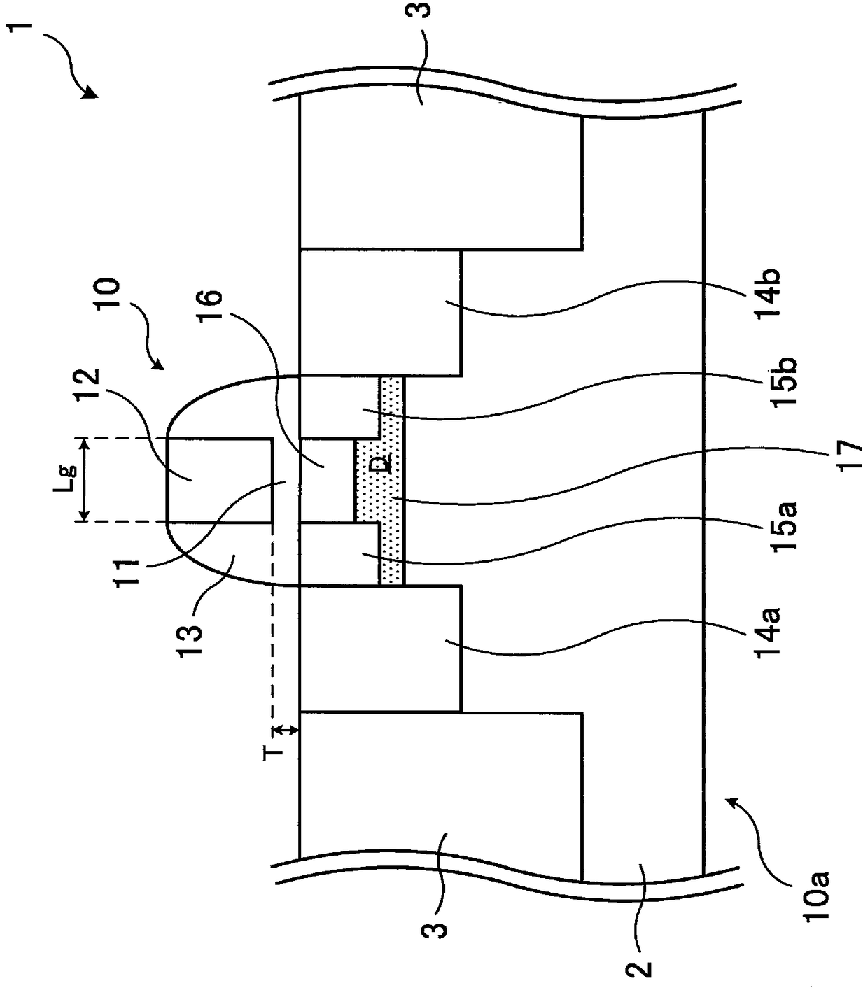
[0042] figure 1 A configuration example of a semiconductor device according to the embodiment is shown. figure 1 A cross-section of relevant components in an example of a semiconductor device according to an embodiment is schematically shown.

[0043] figure 1 The illustrated semiconductor device 1 includes a transistor 10 . Transistor 10 is formed on p-type or n-type semiconductor substrate 2 . Various semiconductor substrates composed of silicon (Si), silicon germanium (SiGe), or the like are used as the semiconductor substrate 2 . A region (element region) 10a where transistor 10 is formed is defined by element isolation region 3 formed on semiconductor substrate 2 by using the STI method or the like.

[0044] Note that although figur...


PUM


Abstract

A semiconductor device includes a first transistor and a second transistor connected to the same power source. Each of the first transistor and the second transistor includes a higher-concentration impurity region of the second conductivity type under the low-concentration channel region disposed between the source region and the drain region of the first conductivity type. The thickness of the gate insulating film of one of the first transistor and the second transistor is made larger than that of the other. According to the present disclosure, off-current in a transistor can be suppressed low.

Description

technical field [0001] Embodiments discussed herein relate to a semiconductor device. Background technique [0002] A technique is known in which a transistor group is used for an internal circuit and a power supply protection circuit to operate a group of MOS (Metal Oxide Semiconductor) type field effect transistors having gates of different thicknesses with the same power supply voltage. electrode insulating film, have different threshold voltages controlled by the impurity concentration in the channel region directly under the gate insulating film, and have different off-state currents. [0003] Also, for a MOS type field effect transistor, a technique is known by forming a channel region that is not doped or has a very low impurity concentration and disposing an impurity concentration higher than that of the channel region under such a channel region. area to control the threshold voltage technique. This technique is expected to be a technique that suppresses variation...

Claims


Application Information

Patent Timeline
Patent Type & Authority Patents(China)
IPC IPC(8): H01L27/088H01L29/06
CPCH01L27/088H01L29/105H01L29/42364H01L29/1083H01L29/7833H01L29/0607H01L21/823493H01L21/823462
Inventor 江间泰示安田真藤田和司
Owner MIE FUJITSU SEMICON
Why Eureka
Try Eureka