Method for producing dual damascene structure

A dielectric layer and semiconductor technology, which is applied in semiconductor/solid-state device manufacturing, electrical components, circuits, etc., can solve the problems that double damascus cannot meet the requirements of forming round corners of through holes and vertical sides of interconnection trenches at the same time. The effect of short eclipse time and avoiding damage

Active Publication Date: 2013-08-14
SEMICONDUCTOR MANUFACTURING INTERNATIONAL (BEIJING) CORP +1
View PDF3 Cites 0 Cited by
  • Summary
  • Abstract
  • Description
  • Claims
  • Application Information

AI Technical Summary

Problems solved by technology

[0035] The object of the present invention is to provide a method for preparing a double damascene structure, so as to solve the problem that the existing method for preparing double damascene can not meet the requirement that the top of the through hole and the bottom of the interconnection trench form a rounded corner and the interconnection trench The problem with these two requirements of lateral verticality

Method used


Image

  • Method for producing dual damascene structure
  • Method for producing dual damascene structure
  • Method for producing dual damascene structure

Examples


Embodiment Construction

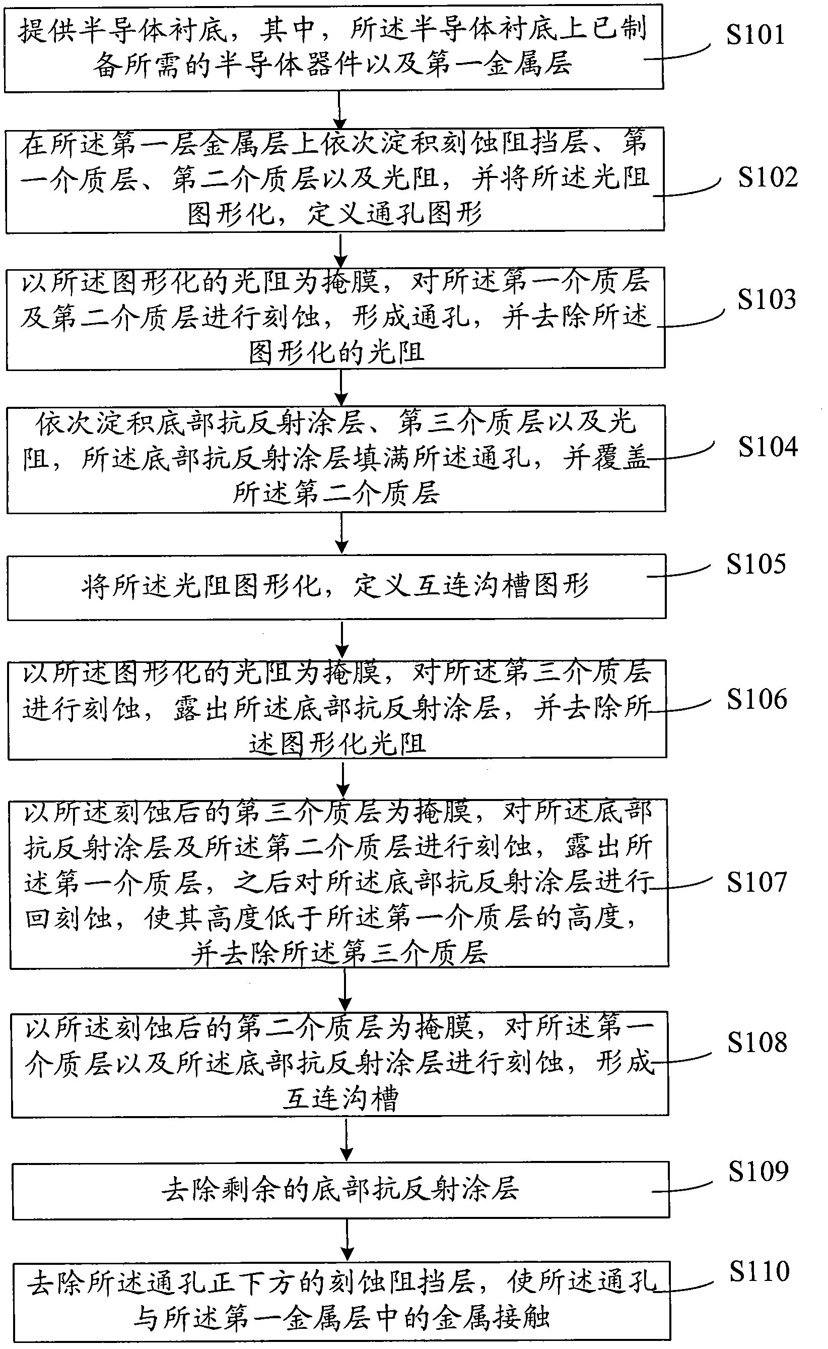
[0076] Please refer to Figure 6 ,as well as Figure 7A to Figure 7J ,in, Figure 6 The flow chart of the method steps for preparing the double damascene structure provided by the embodiment of the present invention, Figure 7A to Figure 7J The schematic diagram of the cross-sectional structure of the device corresponding to each step in the method for preparing the double damascene structure provided by the embodiment of the present invention, as shown in Figure 6 as well as Figure 7A to Figure 7J As shown, the method for preparing a double damascene structure provided by the embodiments of the present invention includes the following steps:

[0077]S301. Provide a semiconductor substrate 301, wherein the required semiconductor device and the first metal layer have been prepared on the semiconductor substrate 301; specifically, the first metal layer includes an inter-metal dielectric layer (IMD, Inter-Metal Dielectric) 302 and the metal 303 in the intermetal dielectric ...


PUM


Abstract

The invention discloses a method for producing a dual damascene structure. The method comprises the following steps of: depositing a part of silicon-containing coating in a through hole; then depositing a bottom antireflective coating; carrying out interconnected groove etching; and when the silicon-containing coating is exposed, introducing CF4, N2 and Ar and continuously etching, or introducingCF4, N2 and Ar for etching and then introducing CF4, N2, Ar and C4F8 and continuously etching. In the environment of the CF4, the N2 and the Ar, the ratio of the etching rate of the silicon-containing coating to the etching rate of a dielectric layer with a low dielectric constant can reach 1.1; in the environment of the CF4, the N2, the Ar and the C4F8, the ratio of the etching rate of the silicon-containing coating to the etching rate of the dielectric layer with the low dielectric constant can reach 3, thereby over etching of the silicon-containing coating is extremely realized when the interconnected groove etching is carried out. Therefore, the method is beneficial to enabling the top of a through hole and the bottom of the interconnected groove to form a circular corner, avoids the damage to the side of the interconnected groove and enables the interconnected groove to keep vertical.

Description

technical field [0001] The invention relates to the technical field of semiconductor devices, in particular to a method for preparing a double damascene structure. Background technique [0002] With the continuous development of integrated circuit manufacturing technology, the characteristic line width of semiconductor chips continues to shrink; at the same time, as the number of transistors in the chip continues to increase and the functions become stronger and stronger, the metal wiring of the chip is getting thinner and thinner. There are more and more layers. This makes the RC delay caused by the connection resistance and the capacitance of the dielectric layer between the connections more and more influential on the chip speed, even exceeding the gate delay that determines the speed of the transistor itself. Therefore, trying to reduce the connection resistance and reduce the capacitance between the connections has become the key to further increase the chip speed. ...

Claims


Application Information

Patent Timeline
Patent Type & Authority Patents(China)
IPC IPC(8): H01L21/768
Inventor 沈满华张海洋周俊卿
Owner SEMICONDUCTOR MANUFACTURING INTERNATIONAL (BEIJING) CORP
Why Eureka
Try Eureka