Liquid crystal display device, process for producing liquid crystal display device, composition for forming polymer layer, and composition for forming liquid crystal layer
一种液晶显示装置、聚合物层的技术,应用在化学仪器和方法、合成树脂层状产品、应用等方向,能够解决液晶分子响应慢、液晶分子传播费时间等问题
- Summary
- Abstract
- Description
- Claims
- Application Information
AI Technical Summary
Problems solved by technology
Method used
Image
Examples
Embodiment approach 1
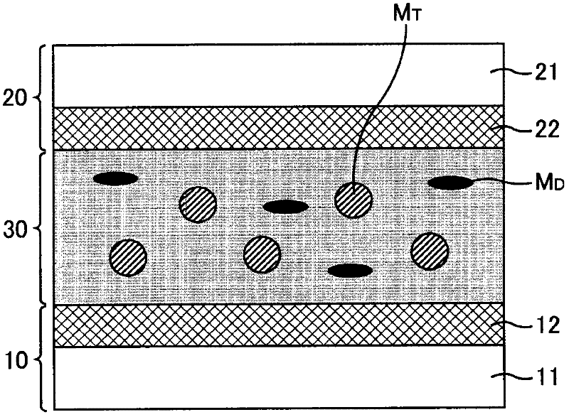
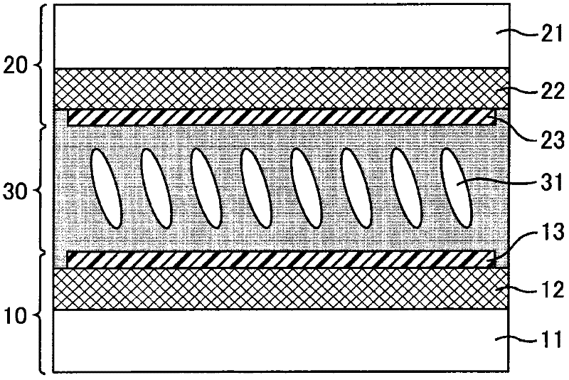
[0063] figure 1 and figure 2 , is a cross-sectional view of the liquid crystal display device according to Embodiment 1. figure 1 Indicates that before the PSA polymerization process, figure 2 Indicates after the PSA polymerization step. Such as figure 1 and figure 2 The illustrated liquid crystal display device according to Embodiment 1 includes an array substrate 10 , a color filter substrate 20 , and a liquid crystal layer 30 sandwiched between a pair of substrates including the array substrate 10 and the color filter substrate 20 . The array substrate 10 has a support substrate 11 including an insulating transparent substrate made of glass or the like, various wirings formed on the transparent substrate, pixel electrodes, TFTs, and the like. The color filter substrate 20 has an insulating transparent substrate made of glass or the like, and a support substrate 21 including a color filter, a black matrix, a common electrode, and the like formed on the transparent su...
Embodiment 1
[0105] Hereinafter, Example 1 in which the liquid crystal cell included in the liquid crystal display device of Embodiment 1 is actually produced is shown. First, prepare a pair of supporting substrates, and coat the surfaces of the pair of substrates respectively, as a material for vertical alignment film, polyamic acid or polyimide solution with photoreactive functional groups in the side chain, at 80°C Prebake at 200°C for 60 minutes.
[0106] Next, from a direction inclined at 45° relative to the surface of the supporting substrate, a 100mJ / cm 2 Irradiation of ultraviolet polarized light having a wavelength near 300 nm was performed to perform photo-alignment treatment.
[0107] Next, a sealant is applied to one support substrate, beads are scattered on the other support substrate, the pair of substrates are attached to each other, and a liquid crystal layer containing a liquid crystal material having a negative dielectric constant anisotropy is injected between the pair ...
Embodiment 2
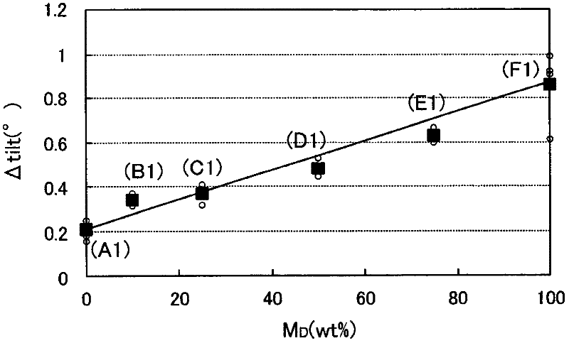
[0122] Example 2 in which the liquid crystal cell included in the liquid crystal display device of Embodiment 1 was actually produced is shown below. In Example 2, except for the polymerizable monomer M T (Monomer for improving pretilt image sticking) and polymerizable monomer M D Each sample was prepared by the same method as in Example 1 except that the material of (the monomer for improving DC image sticking) was different. The polymerizable monomer M of Example 2 T is a compound represented by the following general formula (13), the polymerizable monomer M D It is a compound represented by the following general formula (14).
[0123]
[0124]
[0125] As each sample of Example 2, a polymerizable monomer M was prepared. T The weight ratio and polymerizable monomer M D weight ratio (M T : M D ) is a 9:1 sample (sample B2), a 3:1 sample (sample C2), a 1:1 sample (sample D2), a 1:3 sample (sample E2). In addition, as a reference unit for comparison with the sampl...
PUM
 Abstract
Description
Claims
Application Information
 - R&D
- Intellectual Property
- Life Sciences
- Materials
- Tech Scout
- Unparalleled Data Quality
- Higher Quality Content
- 60% Fewer Hallucinations
Browse by: Latest US Patents, China's latest patents, Technical Efficacy Thesaurus, Application Domain, Technology Topic, Popular Technical Reports.
© 2025 PatSnap. All rights reserved.Legal|Privacy policy|Modern Slavery Act Transparency Statement|Sitemap|About US| Contact US: help@patsnap.com


