
Process for reducing chemical-mechanical polishing crack on buried layer cavity silicon-on-insulator (SOI) wafer

A chemical-mechanical and hollow-type technology, which is applied in the fields of electrical components, semiconductor/solid-state device manufacturing, circuits, etc., can solve problems such as easy deformation or even cracking of the top silicon film, poor consistency of top silicon film thickness, and product quality decline. Achieve the effect of reducing cracking, increasing yield and improving uniformity

Active Publication Date: 2012-01-25
HUNAN RED SUN PHOTOELECTRICITY SCI & TECH
View PDF4 Cites 14 Cited by
  • Summary
  • Abstract
  • Description
  • Claims
  • Application Information

AI Technical Summary

Problems solved by technology

[0006] In order to overcome the defects that the existing SOI wafer preparation process makes the top layer silicon film at the cavity position in the buried layer cavity type SOI wafer easy to deform or even rupture, resulting in poor consistency of the top layer silicon film thickness, decline in product quality or even scrapping, the present invention aims at In providing a process for reducing chemical mechanical grinding cracks of buried layer void type SOI wafers, the process can effectively reduce SiO 2 Breakage of the silicon film on the top layer of SOI wafers with buried voids during the CMP process, improving the SDB (Silicon-silicon Direct Bonding) process, and improving the quality and yield of SOI wafers with buried voids

Method used


Image

  • Process for reducing chemical-mechanical polishing crack on buried layer cavity silicon-on-insulator (SOI) wafer
  • Process for reducing chemical-mechanical polishing crack on buried layer cavity silicon-on-insulator (SOI) wafer
  • Process for reducing chemical-mechanical polishing crack on buried layer cavity silicon-on-insulator (SOI) wafer

Examples


Embodiment Construction

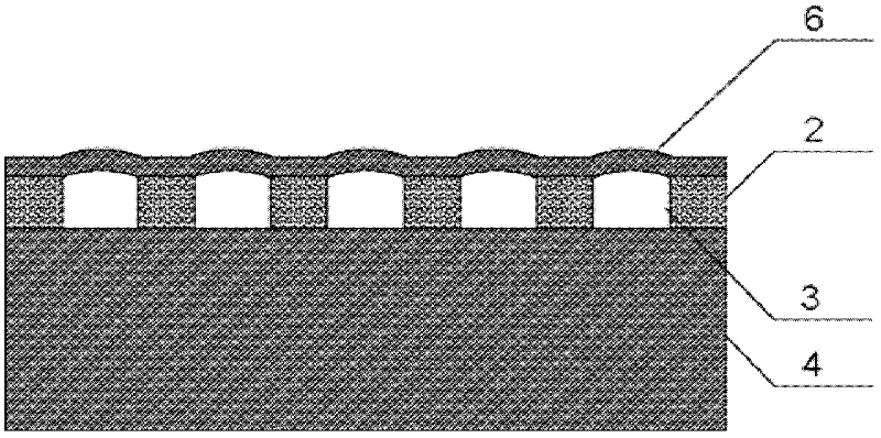
[0039] In order to better understand the process of the present invention, an example is given. The goal is to obtain an SOI wafer with a thickness of the top silicon film 7 of 5 μm and a bonding cavity 3 of 3 μm×3 μm×1 μm. The process flow is as follows: silicon wafer→oxidation→etching→calculation of pressure→bonding→thinning→polishing.

[0040] The semiconductor silicon substrate 4 provided by the present invention takes a P-type silicon wafer as an example, with a thickness of 300 μm and a diameter of 100 mm.

[0041] Step 1: Oxidize a silicon dioxide dielectric layer 2 with a thickness of 1000 nm on the surface of the silicon substrate 4 through a wet oxygen oxidation process. This process actually consumes about 475 nm in thickness of the silicon substrate 4 . The thickness of the silicon dioxide dielectric layer 2 can be used for subsequent formation of the bonding cavity 3 . The typical oxidation temperature is 1050°C, the oxidant is water vapor, and the oxidation t...


PUM

PropertyMeasurementUnit
thicknessaaaaaaaaaa
thicknessaaaaaaaaaa
thicknessaaaaaaaaaa

Abstract

The invention discloses a process for reducing chemical-mechanical polishing cracks on a buried layer cavity silicon-on-insulator (SOI) wafer, belonging to the technical field of microelectronic material processes. Aiming at reducing the thickness of the buried layer cavity SOI wafer through chemical-mechanical polishing, the process mainly comprises the steps of pressure setting, bonding, rough grinding and fine polishing for completing the fabrication of the buried layer cavity SOI wafer. Pressure in a bonding chamber and steps for two stages of chemical-mechanical polishing, i.e. coarse grinding and fine polishing are set according to the final thickness of the top layer silicon film of the SOI wafer. By setting the pressure in the bonding chamber, thermal-induced top layer silicon film deformation in a chemical-mechanical polishing process can be balanced, the cracks on the top layer silicon film of the SOI wafer can be avoided or reduced, the consistency of the thickness of the top layer silicon film is improved, the product quality is controlled very well and the processing cost is reduced.

Description

technical field [0001] The invention relates to a semiconductor material preparation process, in particular to a process for reducing the cracking of a top silicon film during the polishing process of a buried layer cavity type SOI wafer, and belongs to the technical field of microelectronic material technology. Background technique [0002] MEMS technology is developing rapidly, and SOI MEMS technology is getting more and more attention. In SOIMEMS technology, it is often necessary to manufacture patterns in the buried layer structure to form a buried layer void SOI structure, which has led to the development of buried layer void SOI wafer products. Okmetic Company of Finland and IceMOS Company of the United States have begun to sell buried-layer cavity-type SOI wafers (Cavity SOI) products. The 48th Institute of China Electronics Technology Group Corporation, the 24th Institute of China Electronics Technology Group Corporation and Shanghai Simgui Technology have all maste...

Claims


Application Information

Patent Timeline
Patent Type & Authority Applications(China)
IPC IPC(8): H01L21/762H01L21/304
Inventor 颜秀文贾京英朱宗树刘咸成蒋超
Owner HUNAN RED SUN PHOTOELECTRICITY SCI & TECH
Learn More