Method for making storage unit of phase-change random access memory

A phase change memory and memory cell technology, applied in electrical components and other directions, can solve the problems of lower product yield, difficult removal, poor thickness uniformity of the low dielectric constant material layer 105, etc., to achieve the effect of avoiding losses

Active Publication Date: 2013-09-18
SEMICON MFG INT (SHANGHAI) CORP +1
View PDF1 Cites 0 Cited by
  • Summary
  • Abstract
  • Description
  • Claims
  • Application Information

AI Technical Summary

Problems solved by technology

[0012] It should be noted that, in the prior art, due to the thickness of the low dielectric constant material layer 105 that needs to be deposited is relatively thick, about 1 to 2 kiloangstroms, and is limited to the existing deposition and etching technology, the deposited low dielectric constant The thickness uniformity of the material layer 105 is relatively poor, and the thickness uniformity of the low dielectric constant material layer 105 after etching is also relatively poor. There is a remaining silicon nitride layer on the position, that is, the phase change layer 102 will not be etched, so the thickness of the silicon nitride layer 104 deposited in step 12 is also relatively thick, about 400-600 angstroms
Further, since the silicon nitride layer 104 is thicker, its uniformity is also poor. When the silicon nitride layer 104 is etched and the phase change layer 102 is fully exposed, the phase change layer 102 has been etched greatly. a part
On the other hand, since the photoresist layer 106 is used as a mask when etching the low dielectric constant material layer 105, the gas for etching the low dielectric constant material layer 105 is selected. For the low dielectric constant material layer 105 and nitrogen The selection ratio of the silicon oxide layer 104 should not be too high, specifically 1 to 1.5, otherwise heavy polymers (polymers) will be produced during the etching process, which will not be easily removed completely, resulting in some defects, thereby reducing the product yield
Therefore, after the etching of the low dielectric constant material layer 105 is completed, it cannot stop well on the silicon nitride layer 104, that is, a part of the silicon nitride layer 104 will still be etched, if the thickness of the silicon nitride layer 104 is not thick enough. , will then lead to the loss of the phase change layer 102
The phase change layer is the core area of ​​the phase change memory, and this loss is likely to cause the phase change memory unit to not work properly, and the stored information cannot be accurately displayed

Method used


Image

  • Method for making storage unit of phase-change random access memory
  • Method for making storage unit of phase-change random access memory
  • Method for making storage unit of phase-change random access memory

Examples


Embodiment Construction

[0031] In order to make the object, technical solution, and advantages of the present invention clearer, the present invention will be further described in detail below with reference to the accompanying drawings and examples.
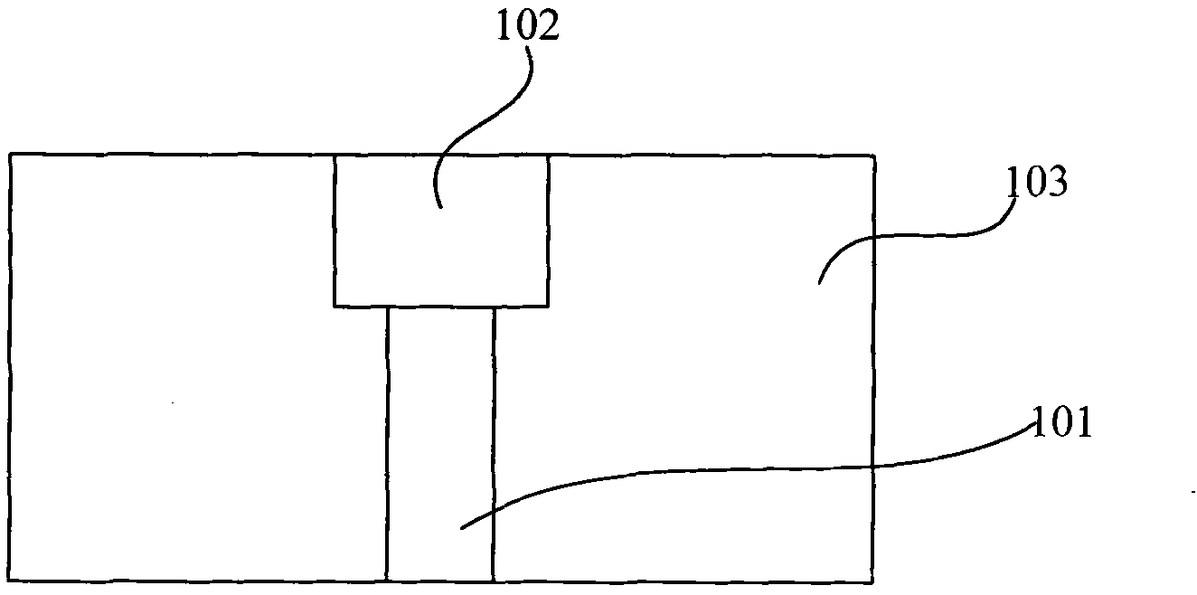
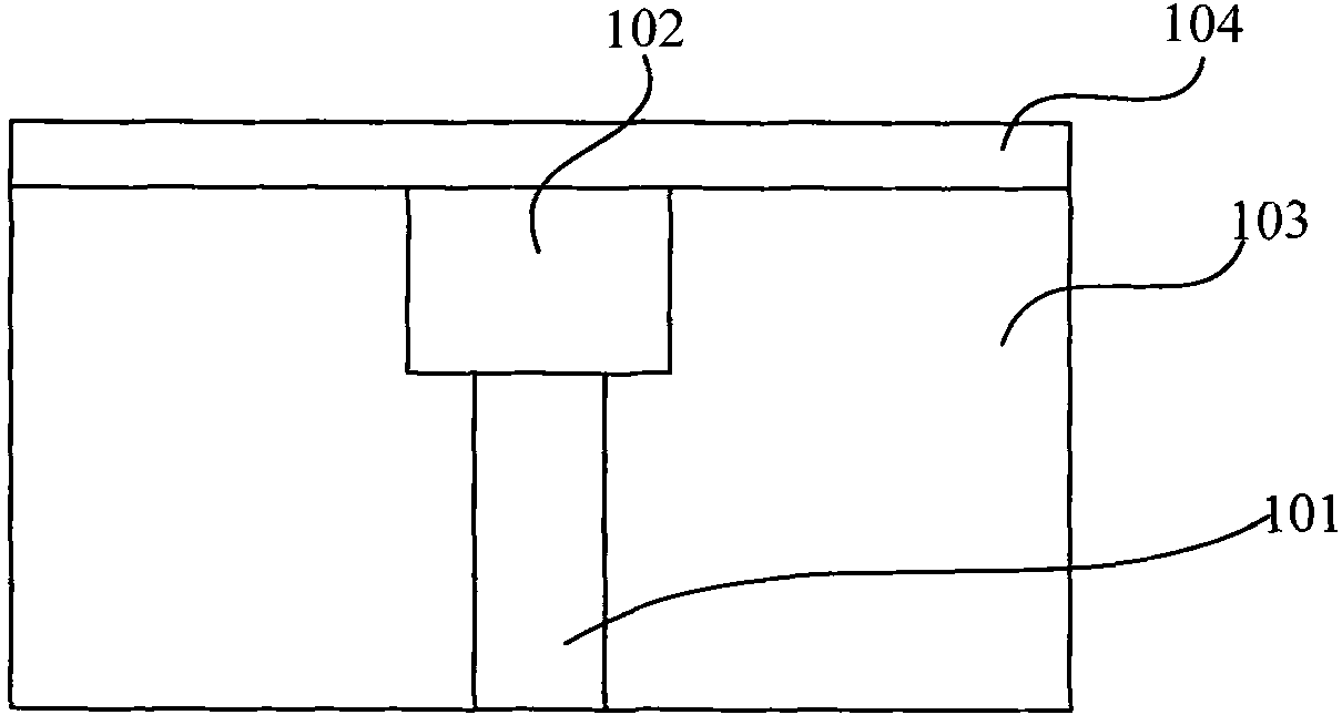
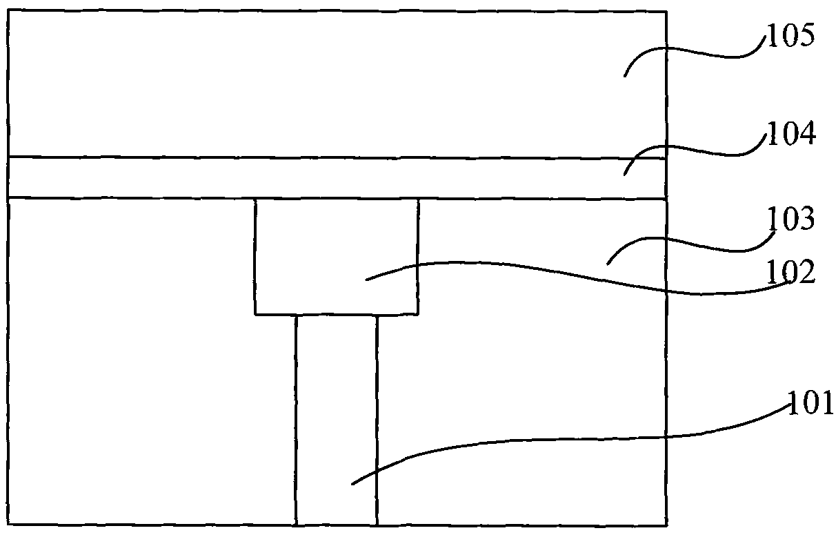
[0032] The core idea of ​​the present invention is to deposit an etch stop layer on the surface of the phase change layer. The etch stop layer is a stack of three layers, which are a nitride layer, an oxide layer and a nitride layer in sequence. Due to the high etching selectivity of the etching gas between the nitride layer and the oxide layer, when etching between adjacent etch stop layers, gradually reduce the etching difference, and finally when the phase change layer is exposed, try to Avoid loss of phase change layer.

[0033] The invention discloses a method for manufacturing a storage unit of a phase-change memory, the schematic flow chart of which is as follows figure 2 As shown, the specific combination of Figure 2a to Figure 2i To illust...


PUM


Abstract

The invention provides a method for making a storage unit of a phase-change random access memory. The method comprises the following steps of: providing a bottom electrode and a phase change layer positioned on the bottom electrode, wherein the bottom electrode and the phase change layer are formed in an insulating layer; depositing three laminated etching stop layers on the surfaces of the phase change layer and the insulating layer, wherein the three laminated etching stop layers sequentially comprise a deposited first nitride layer, an oxide layer and a second nitride layer; sequentially depositing a low-dielectric constant material layer and a coating photoresistive glue layer on the surfaces of the three laminated etching stop layers; exposing, developing and patterning the photoresistive glue layer; defining the position of a top electrode; etching the low-dielectric constant material layer into the three laminated etching stop layers by taking the patterned photoresistive glue layer as a mask and stopping; etching the second nitride layer into the oxide layer and stopping; etching the oxide layer into the first nitride layer and stopping; etching the first nitride layer; and filling an etching position to form the top electrode after the phase change layer is exposed. By the method, the loss of the phase change layer is effectively reduced during etching of the position of the top electrode.

Description

technical field [0001] The invention relates to the technical field of semiconductor manufacturing, in particular to a method for manufacturing a storage unit of a phase-change memory. Background technique [0002] At present, Phase-Change RAM (PC RAM) has non-volatility, long cycle life, small component size, low power consumption, multi-level storage, high-efficiency reading, radiation resistance, high and low temperature resistance, The advantages of anti-vibration, anti-electronic interference and simple manufacturing process are considered to be the most likely to replace the current flash memory (Flash), dynamic random access memory (DRAM) and static memory (SRAM) and become the mainstream product of semiconductor memory in the future. [0003] A PC RAM memory cell includes a phase change layer, and bottom and top electrodes in contact with the phase change layer. The phase change layer of the PC RAM storage unit is the core area of ​​the phase change memory, which is...

Claims


Application Information

Patent Timeline
Patent Type & Authority Patents(China)
IPC IPC(8): H01L45/00
Inventor 洪中山
Owner SEMICON MFG INT (SHANGHAI) CORP
Why Eureka
Try Eureka