Manufacturing process of silicon heterojunction solar battery

A solar cell and heterojunction technology, which is applied in the manufacture of circuits, electrical components, and final products, can solve problems such as uneven film thickness, difficult film formation, and difficult concentration control, and achieve the effect of avoiding uneven film thickness

Inactive Publication Date: 2012-01-11
NATIONAL TSING HUA UNIVERSITY
View PDF5 Cites 1 Cited by
  • Summary
  • Abstract
  • Description
  • Claims
  • Application Information

AI Technical Summary

Problems solved by technology

When the film is very thin (such as a few nanometers), it is difficult to form a film by plasma-enhanced chemical vapor deposition. Not only is the concentration of doping difficult to control, but it is also prone to problems of uneven film thickness or failure to form a film in some areas.

Method used


Image

  • Manufacturing process of silicon heterojunction solar battery
  • Manufacturing process of silicon heterojunction solar battery
  • Manufacturing process of silicon heterojunction solar battery

Examples


Embodiment Construction

[0013] Relevant detailed description and technical content of the present invention, now coordinate drawing description as follows:

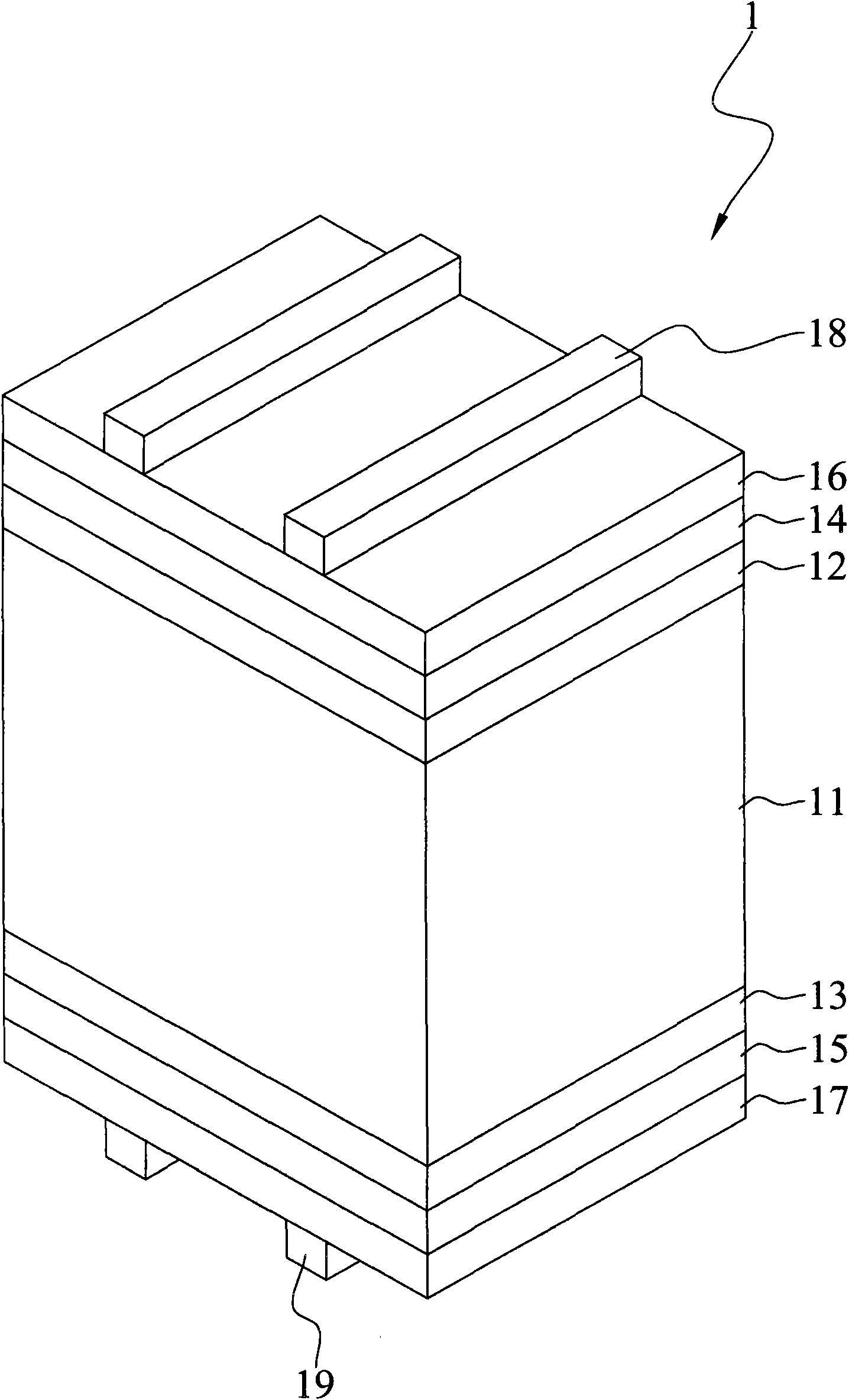
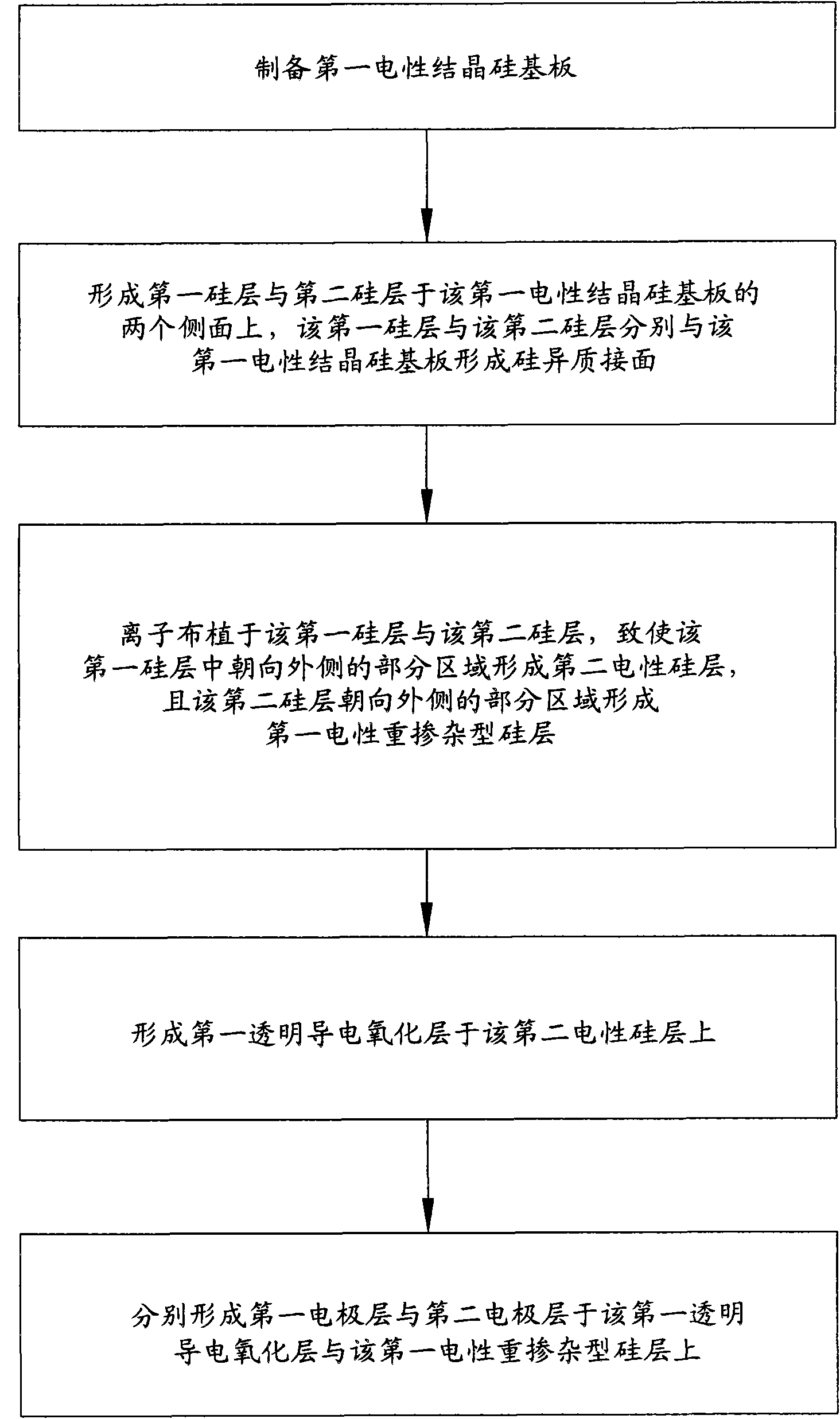
[0014] refer to figure 2 As shown, it is a flowchart of an embodiment of the present invention, as shown in the figure: the present invention proposes a process for manufacturing a silicon heterojunction solar cell, the steps of which include: preparing a first electrical crystalline silicon substrate; forming a second A silicon layer and a second silicon layer are on two sides of the first electrical crystalline silicon substrate, and the first silicon layer and the second silicon layer respectively form silicon heterojunctions with the first electrical crystalline silicon substrate ; Ions are implanted in the first silicon layer and the second silicon layer, so that the outer part of the first silicon layer forms the second electrical silicon layer, and the outer part of the second silicon layer forms the first silicon layer. An electrical h...


PUM


Abstract

The invention relates to a manufacturing process of a silicon heterojunction solar battery. The silicon heterojunction solar battery comprises a first electric silicon substrate, a first intrinsic silicon layer, a second intrinsic silicon layer, a second electric silicon layer and a first electric heavily-doping silicon layer, wherein the first intrinsic silicon layer and the second intrinsic silicon layer are respectively formed at two sides of the first electric silicon substrate and forms a heterojunction with the first electric silicon substrate; and the second electric silicon layer and the first electric heavily-doping silicon layer are respectively formed on the first intrinsic silicon layer and the second intrinsic silicon layer. According to the invention, the second electric silicon layer and the first electric heavily-doping silicon layer are formed in an ion implantation way so as to optimize the thicknesses and the doping qualities of the second electric silicon layer and the first electric heavily-doping silicon layer.

Description

technical field [0001] The invention relates to a manufacturing process of a silicon heterojunction solar cell, in particular to a manufacturing process of a silicon heterojunction solar cell that reduces manufacturing costs and improves conversion efficiency. Background technique [0002] With the development of science and technology, the evolution of civilization and the rapid growth of population, the use and consumption of energy is increasing day by day. In the case of limited natural resources such as oil, natural gas and coal, how to save energy and find and develop alternative energy has become one of the most important issues to be solved and cannot be ignored. Since the energy from the sun is large and inexhaustible, the development of solar cells as devices for power generation and storage has gradually become the mainstream in the new century. [0003] A so-called solar cell is a photovoltaic component that converts the sun's energy into electricity. The simpl...

Claims


Application Information

Patent Timeline
Patent Type & Authority Applications(China)
IPC IPC(8): H01L31/18
CPCY02P70/50
Inventor 杨士贤吴永俊
Owner NATIONAL TSING HUA UNIVERSITY
Why Eureka
Try Eureka