
Multi-finger strip-type gate-ground N-channel metal oxide semiconductor (GGNMOS) and electrostatic protection circuit

A strip, N-type technology, applied in circuits, electrical components, electrical solid devices, etc., can solve the problems of poor conduction uniformity of GGNMOS parallel structure, poor conduction uniformity, parasitic NPN transistors cannot be turned on and discharged at the same time, etc. Achieve the effect of improving conduction uniformity

Active Publication Date: 2012-01-11
SHANGHAI HUAHONG GRACE SEMICON MFG CORP
View PDF4 Cites 7 Cited by
  • Summary
  • Abstract
  • Description
  • Claims
  • Application Information

AI Technical Summary

Problems solved by technology

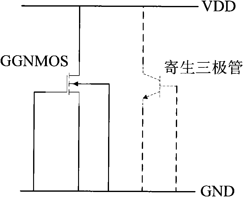
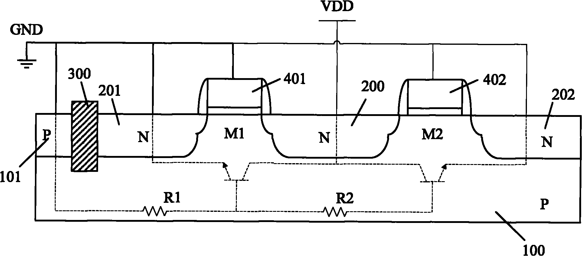
According to the known principle, the triode with the same potential difference between the collector and the emitter and the same specification, the greater the potential difference between the base and the emitter, the easier it is to conduct, so when the electrostatic damage on the power line VDD causes the potential to rise , the NPN transistor T2 is always turned on before the NPN transistor T1, which makes the conduction uniformity of the above-mentioned multi-tube GGNMOS parallel structure very poor
Poor conduction uniformity will cause the following problems: all the parasitic NPN transistors cannot be turned on and discharged at the same time. When the parasitic NPN transistor T1 is turned on, the NPN transistor T2, that is, the second NMOS M2, may be over due to the excessive applied voltage. be damaged

Method used


Image

  • Multi-finger strip-type gate-ground N-channel metal oxide semiconductor (GGNMOS) and electrostatic protection circuit
  • Multi-finger strip-type gate-ground N-channel metal oxide semiconductor (GGNMOS) and electrostatic protection circuit
  • Multi-finger strip-type gate-ground N-channel metal oxide semiconductor (GGNMOS) and electrostatic protection circuit

Examples


Embodiment Construction

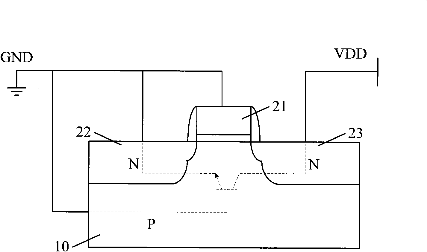
[0024] In the existing multi-finger strip GGNMOS, the parasitic internal resistance between the base and the ground of each parasitic NPN transistor is different, resulting in different base potentials of each parasitic NPN transistor, that is, the potential difference between the base and the emitter. The same, so the conduction uniformity is poor. When a voltage is applied to the drain, that is, the collector of the parasitic NPN transistor, each parasitic NPN transistor cannot be turned on at the same time, so part of the GGNMOS may be damaged. In the present invention, an N-type connection well is arranged between the drains of adjacent NMOS transistors in a multi-finger strip GGNMOS, thereby forming a parasitic internal resistance between the drain and an external circuit, and adjusting the N-type connection well surface area. The position of the N-type connection region can change the size of the parasitic internal resistance, thereby adjusting and improving the conductio...


PUM


Abstract

The invention provides a multi-finger strip-type gate-ground N-channel metal oxide semiconductor (GGNMOS) and an electrostatic protection circuit. The multi-finger strip-type GGNMOS comprises a P-type semiconductor substrate, at least two N-channel metal oxide semiconductor (NMOS) transistors formed in a device region, and an N-type connecting pit positioned in a semiconductor substrate arranged between drains of adjacent NMOS transistors; the P-type semiconductor substrate comprises the device region; the N-type connecting pit is connected with the drains on the two sides of the N-type connecting pit; and an N-type connecting region is formed in a surface region of the N-type connecting pit. The multi-finger strip-type GGNMOS provided by the invention has high conduction uniformity.

Description

technical field [0001] The invention relates to the design field of integrated circuit electrostatic protection circuits, in particular to a multi-finger bar-shaped GGNMOS and electrostatic protection circuit. Background technique [0002] Integrated circuits are easily subject to destructive electrostatic discharge (ESD) during manufacture, assembly, testing or final application, causing the integrated circuits to be damaged by static electricity. Therefore, usually in an integrated circuit, an ESD protection circuit is formed, that is, a discharge unit that can discharge static electricity on the I / O pad is coupled to the input / output pad (I / O pad), thereby reducing the impact of static electricity on the integrated circuit. caused damage. Under the current CMOS process, the most commonly used ESD protection circuit structure is usually based on gate-grounded NMOS (Gate-ground NMOS, GGNMOS). [0003] figure 1 is a schematic circuit diagram of an existing single-tube str...

Claims


Application Information

Patent Timeline
Patent Type & Authority Applications(China)
IPC IPC(8): H01L27/088H01L29/06H01L27/04
Inventor 单毅陈晓杰
Owner SHANGHAI HUAHONG GRACE SEMICON MFG CORP
Learn More