A method for encapsulating an optoelectronic device
A technology of optoelectronic devices and packaging methods, which is applied in the field of optoelectronics, can solve the problems of black spots, decreased stability, and decreased device performance, and achieve the effects of prolonging device life, good curing agent properties, and improving device stability
- Summary
- Abstract
- Description
- Claims
- Application Information
AI Technical Summary
Problems solved by technology
Method used
Image
Examples
Embodiment 1
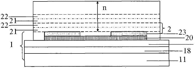
[0032] Such as figure 1 As shown, 1 is an organic electroluminescent device, the anode layer 12 is ITO, and the hole transport layer 13 is N, N'-bis(naphthylidene-1-yl)-N,N'-bis(phenyl) - benzidine (NPB), electron transport layer 14 is 1,3,5-(tri-N-phenyl-2-benzimidazole-2) benzene 41 (TPBi), cathode layer 15 is Mg:Ag alloy, inorganic thin film Packaging material layer 21 is Al 2 o 3 , UV-curable resin 22 includes 75% epoxidized octadecanoconjugated triene-9,11,13-acid triglyceride, 15% reaction diluent and 10% triaryl sulfur type hexafluorophosphonium salt , the number of cycles n is 20, and the device structure is:
[0033] Glass substrate / ITO / NPB(50nm) / TPBi(30nm) / Mg:Ag(200nm) / [Al 2 o 3 (200nm) / UV curable resin (100nm)] 20
[0034] The preparation method is as follows:
[0035] ①Use detergent, acetone solution, ethanol solution and deionized water to ultrasonically clean the substrate and dry it with nitrogen;
[0036] ②Transfer the clean substrate to the high vacuu...
Embodiment 2
[0043] Such as figure 1 As shown, 1 is an organic electroluminescent device, the anode layer 12 is ITO, and the hole transport layer 13 is N, N'-bis(naphthylidene-1-yl)-N,N'-bis(phenyl) - benzidine (NPB), electron transport layer 14 is 1,3,5-(tri-N-phenyl-2-benzimidazole-2) benzene 41 (TPBi), cathode layer 15 is Mg:Ag alloy, inorganic thin film Packaging material layer 21 is Al 2 o 3 , UV-curable resin 22 includes 82% epoxidized octadecanoconjugated triene-9,11,13-acid triglyceride, 10% reactive diluent and 8% triarylsulfur-type hexafluorophosphorus salt , the number of cycles n is 16, and the device structure is:
[0044] Glass substrate / ITO / NPB(50nm) / TPBi(30nm) / Mg:Ag(200nm) / [Al 2 o 3 (200nm) / UV curable resin (100nm)] 16
[0045] The preparation method is similar to Example 1.
Embodiment 3
[0047] Such as figure 1 As shown, 1 is an organic electroluminescent device, the anode layer 12 is ITO, and the hole transport layer 13 is N, N'-bis(naphthylidene-1-yl)-N,N'-bis(phenyl) - benzidine (NPB), electron transport layer 14 is 1,3,5-(tri-N-phenyl-2-benzimidazole-2) benzene 41 (TPBi), cathode layer 15 is Mg:Ag alloy, inorganic thin film Packaging material layer 21 is Al 2 o 3 , UV-curable resin 22 includes 90% epoxidized octadecanoconjugated triene-9,11,13-acid triglyceride, 5% reactive diluent and 5% triarylsulfur-type hexafluorophosphorus salt , the number of cycles n is 12, and the device structure is:
[0048] Glass substrate / ITO / NPB(50nm) / TPBi(30nm) / Mg:Ag(200nm) / [Al 2 o 3 (200nm) / UV curable resin (100nm)] 12
[0049] The preparation method is similar to Example 1.
PUM
 Abstract
Description
Claims
Application Information
 - R&D
- Intellectual Property
- Life Sciences
- Materials
- Tech Scout
- Unparalleled Data Quality
- Higher Quality Content
- 60% Fewer Hallucinations
Browse by: Latest US Patents, China's latest patents, Technical Efficacy Thesaurus, Application Domain, Technology Topic, Popular Technical Reports.
© 2025 PatSnap. All rights reserved.Legal|Privacy policy|Modern Slavery Act Transparency Statement|Sitemap|About US| Contact US: help@patsnap.com


