Plasma processing apparatus, substrate holding mechanism, and positional deviation detection method

A substrate holding and offset detection technology, applied in the direction of using fluid devices, measuring devices, semiconductor/solid-state device testing/measurement, etc., can solve the problems of inability to detect the positional deviation of semiconductor wafers, inability to detect positional deviation, etc. , to achieve the effect of improving the accuracy of position offset detection and eliminating pressure loss

Active Publication Date: 2011-12-28
TOKYO ELECTRON LTD
View PDF4 Cites 18 Cited by
  • Summary
  • Abstract
  • Description
  • Claims
  • Application Information

AI Technical Summary

Problems solved by technology

In this method, for example, when there is no semiconductor wafer or the electrostatic holding force is small, the pressure measurement gas leaks from the pressure measurement hole and the pressure drops. Therefore, by monitoring the pressure, it is possible to detect the presence of the semiconductor wafer on the mounting table. None and hold state, but cannot detect the positional deviation of the semiconductor wafer
The technique described in Patent Document 2 also provides a pressure measurement hole on the upper part of the mounting table to detect pressure, but it cannot detect positional displacement similarly to the above.

Method used


Image

  • Plasma processing apparatus, substrate holding mechanism, and positional deviation detection method
  • Plasma processing apparatus, substrate holding mechanism, and positional deviation detection method
  • Plasma processing apparatus, substrate holding mechanism, and positional deviation detection method

Examples


Embodiment Construction

[0039] Preferred embodiments of the present invention will be described in detail below with reference to the drawings. In addition, in this specification and drawings, the same code|symbol is attached|subjected to the component which has substantially the same functional structure, and repeated description is abbreviate|omitted.

[0040] (Example of structure of plasma processing apparatus)

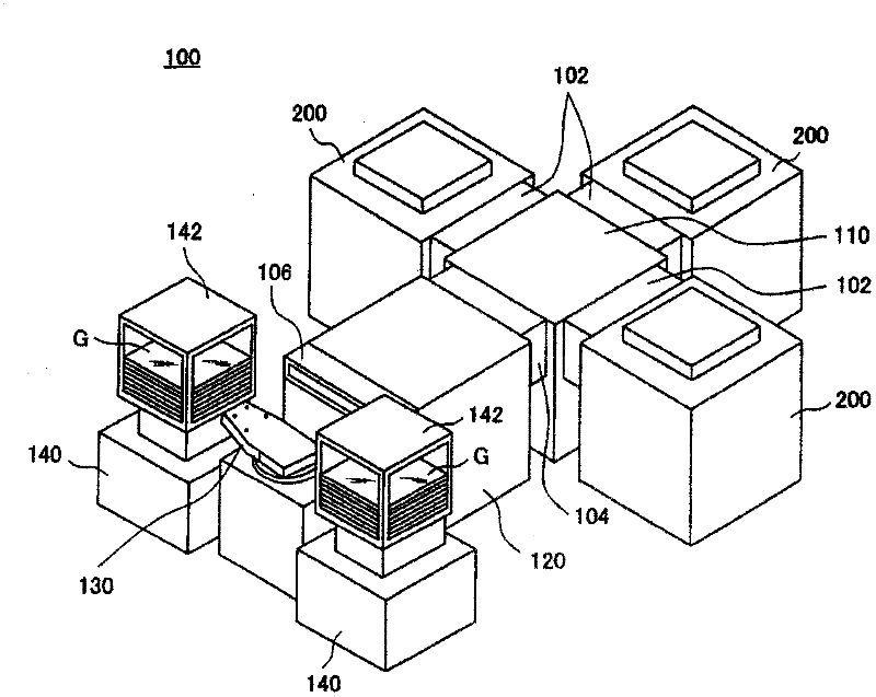
[0041] First, an embodiment in which the present invention is applied to a multi-chamber processing apparatus having a plasma processing apparatus will be described with reference to the drawings. figure 1 It is an external perspective view of the processing apparatus 100 of this embodiment. The processing apparatus 100 shown in this figure has three plasma processing apparatuses for performing plasma processing on the substrate for flat panel display (substrate for FPD) G. Each plasma processing apparatus has a processing chamber 200 .

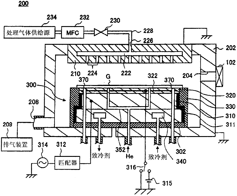
[0042] In the processing chamber 200, for exa...


PUM


Abstract

The invention provides a plasma processing apparatus, a substrate holding mechanism, and a method for the substrate position deviation detection. The influence of the pressure loss of a gas flow path of a heat transfer gas can be eliminated, and the precision of the substrate position deviation detection is also improved. The plasma processing apparatus is provided with the gas flow path (352) of the gas from a gas supply source. And the gas flow path is arranged between to-be-processed substrates kept on a substrate keeping surface and gives the gas to a carrying platform (300). The substrate keeping surface formed on the carrying platform introduces the gas from the gas flow path into a plurality of pores (354) in the substrate keeping surface (Ls). A plurality of pressure detecting holes (370a to 370 d) which are used to detect the pressure on a rear side of the substrate are formed at the outside of a pore forming area (R) of the substrate keeping surface. Pressure sensors (380a to 380 d) which are connected with the pressure detecting holes are also included. The substrate position deviation detection is carried out based on the detection pressure of the pressure sensors.

Description

technical field [0001] The present invention relates to a plasma processing apparatus, a substrate holding mechanism, and a method for detecting a positional deviation of a substrate for performing plasma processing on a large substrate such as a glass substrate for a flat panel display (FPD). Background technique [0002] In FPD panel manufacturing, pixel designs, electrodes, wiring, etc. are generally formed on a substrate made of an insulator such as glass. Among various processes of such panel production, microprocessing such as etching, CVD, ashing, and sputtering is performed by a plasma processing apparatus. In a plasma processing apparatus, for example, a substrate is placed on a stage having a susceptor constituting a lower electrode in a decompressible processing chamber, and high-frequency power is supplied to the susceptor to form plasma of a processing gas on the substrate. This plasma performs predetermined processing such as etching on the substrate. [0003...

Claims


Application Information

Patent Timeline
Patent Type & Authority Applications(China)
IPC IPC(8): H01L21/683H01L21/00G01B13/00H01L21/66
CPCH01J37/32715H01L21/67017H01L21/67253H01L21/687H01L22/12
Inventor 东条利洋古屋敦城
Owner TOKYO ELECTRON LTD
Why Eureka
Try Eureka