An array type optical addressable potential sensor and its manufacturing method

A potential sensor and manufacturing method technology, applied in the direction of material electrochemical variables, etc., can solve the problems of unfavorable array photo-addressable potential sensor miniaturization and integration, unsatisfactory noise suppression effect, photoresist cannot be soaked for a long time, etc. Achieve the effect of being conducive to miniaturization, reducing volume and improving test accuracy

Inactive Publication Date: 2011-12-21
ZHEJIANG UNIV
View PDF2 Cites 5 Cited by
  • Summary
  • Abstract
  • Description
  • Claims
  • Application Information

AI Technical Summary

Problems solved by technology

These methods have inherent defects: polyimide and photoresist will pollute the sensitive unit during the photolithography process, and the photoresist still has the limitation that it cannot be soaked in the solution for a long time. Although there is no corresponding pollution in the thick oxide layer, the The noise suppression effect is not ideal
At the same time, the reference electrode on the current array optical addressable potential sensor basically adopts the traditional larger Ag / AgCl electrode or calomel electrode, which is not conducive to the miniaturization and integration of the array optical addressable potential sensor.

Method used


Image

  • An array type optical addressable potential sensor and its manufacturing method
  • An array type optical addressable potential sensor and its manufacturing method
  • An array type optical addressable potential sensor and its manufacturing method

Examples


Embodiment Construction

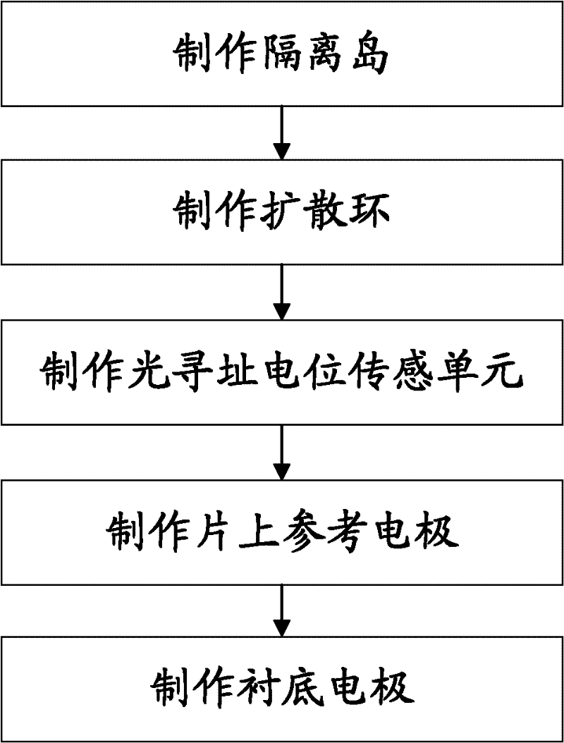
[0032] In order to describe the present invention in more detail, the technical solution of the present invention will be described in detail below with reference to the accompanying drawings and specific embodiments.

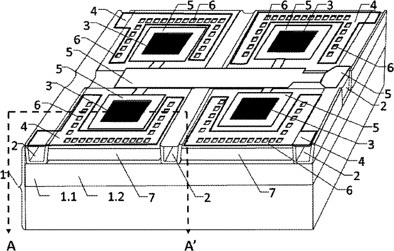
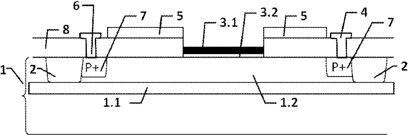
[0033] Such as figure 1 with figure 2 As shown, a 2×2 array optical addressable potential sensor includes an SOI substrate 1 and four isolation islands formed on the SOI substrate 1;

[0034] The SOI substrate 1 is provided with a silicon dioxide layer 8; the isolation island is composed of the buried oxide layer 1.1 of the SOI substrate 1 and the top silicon 1.2 provided on the SOI substrate 1 and connects the silicon dioxide layer 8 and the buried oxide layer 1.1 A ring-shaped isolation groove 2 is formed; the adjacent sides of the ring-shaped isolation groove 2 of two adjacent isolation islands merge;

[0035] A P+ diffusion ring 7 is provided on the top of the top silicon 1.2 in the isolation island, and the P+ diffusion ring 7 is connected to the annular isolati...


PUM

PropertyMeasurementUnit
thicknessaaaaaaaaaa
electrical resistivityaaaaaaaaaa

Abstract

The invention discloses an array-type light addressable potentiometric sensor comprising an SOI (Silicon-On-Insulator) substrate and a plurality of isolating islands formed on the SOI substrate, wherein the SOI substrate in the isolating islands is provided with light addressable potentiometric sensing units, a diffusion ring, a substrate electrode and an on-chip reference electrode. The invention further discloses a manufacturing method of the array-type light addressable potentiometric sensor, and the method comprises the steps of: (1) manufacturing the isolating islands; (2) manufacturing the diffusion ring; (3) manufacturing the light addressable potentiometric sensing units; (4) manufacturing the on-chip reference electrode; and (4) manufacturing the substrate electrode. According tothe invention, the degree of isolation between the light addressable potentiometric sensing units are effectively enhanced by adopting the SOI substrate in combination with the isolation channel groove, and the unique design of the on-chip reference electrode in the invention is more favorable for the microminiaturization and integration of the sensor.

Description

Technical field [0001] The invention belongs to the technical field of sensor design, and specifically relates to an array type light addressing potential sensor and a manufacturing method thereof. Background technique [0002] Light Addressable Potential Sensor (LAPS) is a sensor device based on capacitive sensor combined with photoelectric characteristics of semiconductor. Because of its simple preparation process, low packaging requirements, good potential stability, high sensitivity, short response time, and movable light source during measurement, it has caused extensive research and applications. [0003] The sensitive unit of the light-addressable potential sensor has an electrolyte solution-sensitive film-semiconductor structure. When the semiconductor surface of the photo-addressable potential sensor is biased in the depleted state, the light source with adjustable intensity is used to illuminate the silicon wafer, and the photons will excite the silicon material electron...

Claims


Application Information

Patent Timeline
Patent Type & Authority Applications(China)
IPC IPC(8): G01N27/26
Inventor 孙颖朱大中郭维
Owner ZHEJIANG UNIV
Why Eureka
Try Eureka