Device for scraping and cutting on semiconductor device chip glass passive film and using method thereof

A glass passivation, device chip technology, applied in welding equipment, laser welding equipment, metal processing equipment, etc.

Active Publication Date: 2013-11-13
JIANGSU JIEJIE MICROELECTRONICS
View PDF9 Cites 0 Cited by
  • Summary
  • Abstract
  • Description
  • Claims
  • Application Information

AI Technical Summary

Problems solved by technology

[0004]1. Grinding wheel scribing belongs to the contact scribing method. During the scribing process, the silicon wafer is easily subjected to mechanical stamping force, and the silicon wafer is easily deformed and displaced, resulting in semiconductor Chips are scrapped due to broken edges and deflected scratches
[0005]2. The speed of the grinding wheel blade is very slow when cutting the glass passivation film of the semiconductor device chip (generally around ≤8mm / s), and the production efficiency is extremely low. After that, there are many cracks, and the surface of the device chip contains dust attached, which seriously affects the product characteristics
[0006]3. Grinding wheel scribing requires more consumable auxiliary materials, such as: a large amount of deionized water, grinding wheel blades, trimming blades, auxiliary tools, etc., required maintenance costs, High labor cost

Method used


Image

  • Device for scraping and cutting on semiconductor device chip glass passive film and using method thereof
  • Device for scraping and cutting on semiconductor device chip glass passive film and using method thereof

Examples


Embodiment 1

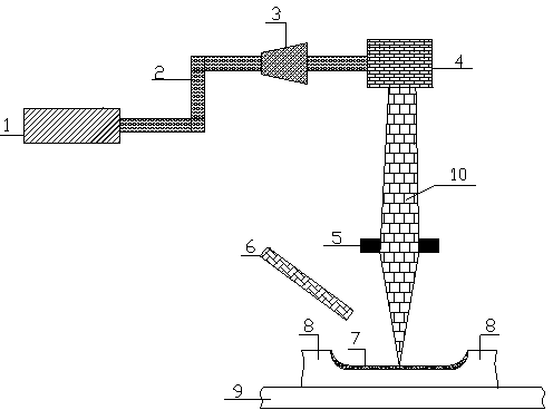
[0032] Such as figure 1 As shown, the device of the present invention for scribing on the glass passivation film of a semiconductor device chip includes a laser 1 capable of generating a violet laser beam 10, an optical transmission channel 2 for the optical transmission of the violet laser beam 10, and diverging the violet laser beam 10. The beam expander 3, the deflection device 4 that changes the parallel direction of the violet laser beam 10, the optical focusing device 5 that focuses the divergent violet laser beam 10, and the blowing exhaust device that blows away the dust generated during the scribing process 6. Protect the glass passivation film 7 on the surface of the single-table semiconductor device chip and the operating platform 9 for placing the single-table semiconductor device chip 8, the laser 1 is connected to the optical transmission channel 2, and the beam expander 3 and the deflection device 4 are set On the optical transmission channel 2 , the optical fo...

Embodiment 2

[0045] Such as figure 1 As shown, the structure of the device of the present invention for scribing on the glass passivation film of the semiconductor device chip is the same as that of Embodiment 1.

[0046] The above-mentioned scribing device performs scribing on a single-mesa semiconductor device chip with a thickness of 300 μm, and its use method includes the following steps:

[0047] a. First adjust the crystal temperature value by 0.1°C each time, and measure the power value with a power measuring device to find the crystal temperature value suitable for the normal operation of the crystal to be 25°C. At the same time, ensure that the temperature and humidity of the working environment are stable, and ensure that the laser 1 works normally and stably;

[0048] b. Adjust the horizontal polarizer of the optical transmission channel 2 to ensure that the violet laser beam 10 is horizontal from the laser emission hole to the entrance of the beam expander 3;

[0049] c. Adju...

Embodiment 3

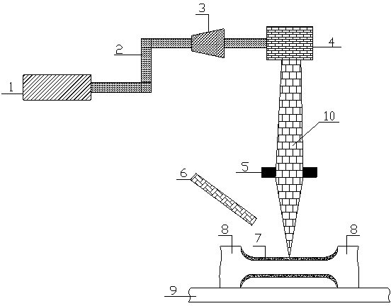
[0058] Such as figure 2 As shown, the device of the present invention for scribing on the glass passivation film of a semiconductor device chip includes a laser 1 capable of generating a violet laser beam 10, an optical path transmission channel 2 for the optical path transmission of the violet laser beam, and a beam expander for diverging the violet laser beam Device 3. The deflection device for changing the parallel direction of the purple laser beam 10. 4. The optical focusing device for focusing the divergent purple laser beam. The glass passivation film 7 on the surface of the mesa semiconductor device chip 8 and the operating platform 9 on which the double mesa semiconductor device chip 8 is placed, the laser 1 is connected to the optical transmission channel 2, the beam expander 3 and the deflection device 4 are placed on the optical transmission On the channel 2 , the optical focusing device 5 is arranged on both sides of the violet laser beam 10 , and the air blowing...


PUM

PropertyMeasurementUnit
thicknessaaaaaaaaaa
thicknessaaaaaaaaaa
thicknessaaaaaaaaaa

Abstract

The invention discloses a device for scraping and cutting on a semiconductor device chip glass passive film. The device is characterized by comprising a laser, a light path transmission channel, a beam-expanding device, a deflection device, an optical focusing device, an air blowing and exhausting device, a glass passive film and an operating platform, wherein the laser is connected with the light path transmission channel; the optical focusing device is arranged on two sides of a purple light laser beam; and the air blowing and exhausting device is arranged on one side of the purple light laser beam. The invention also discloses a using method of the scraping and cutting device. The using method comprises the following steps of: adjusting the temperature value of a crystal; adjusting a horizontal polarizer of the light path transmission channel; adjusting and fixing the position of the beam-expanding device; adjusting the deflection device; arranging and adjusting the optical focusing device; adjusting and testing the horizontal angle of the operating platform; adjusting the working Q frequency and electric frequency pulse width of the laser; selecting proper current and scraping and cutting speed; and inspecting products. The device and the using method thereof have the advantages of high scraping and cutting speed, low consumption cost, low maintenance cost, high productivity and high silicon wafer area utilization ratio.

Description

technical field [0001] The invention relates to a method for using a device for scribing on a semiconductor device chip glass passivation film. Background technique [0002] In the semiconductor device chip scribing process, the method of scribing with a grinding wheel blade in the slicing area on the silicon material between the chip and the chip is generally used: the silicon chip to be diced is attached to the blue film, and the high-speed rotating The grinding wheel blade cuts the silicon wafer in the vertical and horizontal directions, and then stretches the blue film to separate the semiconductor device chips from each other, which is convenient for the subsequent packaging of the finished product. [0003] There are following deficiencies in the method of grinding wheel scribing: [0004] 1. Grinding wheel scribing is a contact scribing method. During the scribing process, the silicon wafer is easily subjected to mechanical punching force, and the silicon wafer is ea...

Claims


Application Information

Patent Timeline
Patent Type & Authority Patents(China)
IPC IPC(8): B23K26/36B23K26/14B23K26/38
Inventor 王琳周榕榕
Owner JIANGSU JIEJIE MICROELECTRONICS
Why Eureka
Try Eureka