Led device with light extracting rough structure and manufacturing methods thereof

A technology for light-emitting diodes and a manufacturing method, which is applied to lighting devices, components of lighting devices, lighting and heating equipment, etc., can solve problems such as reducing light-emitting efficiency of light-emitting diodes

Inactive Publication Date: 2011-11-23
SEMILEDS OPTOELECTRONICS CO LTD
View PDF4 Cites 6 Cited by
  • Summary
  • Abstract
  • Description
  • Claims
  • Application Information

AI Technical Summary

Problems solved by technology

like figure 1 As shown, the light-emitting diode 110 is covered by the lens 120, and when the light-emitting diode 110 emits light, the light emitted by it can reach the surface 125 of the lens 120, and at this time, the light may pass through the lens surface 125 and emit to the outside world (as shown by arrow A), or, total reflection occurs on the lens surface 125 and turns back to the inside of lens 120 (as shown by arrow B), thereby reducing the light-emitting efficiency of the light-emitting diode

Method used


Image

  • Led device with light extracting rough structure and manufacturing methods thereof
  • Led device with light extracting rough structure and manufacturing methods thereof
  • Led device with light extracting rough structure and manufacturing methods thereof

Examples


Embodiment Construction

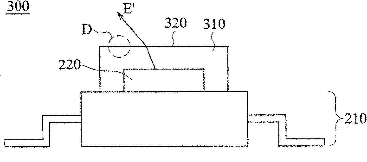
[0050] figure 2 A schematic diagram of a light emitting diode device 200 with a roughened light output structure according to an embodiment of the present invention is shown. Such as figure 2 As shown, the LED device 200 includes: a lead frame 210 ; an LED chip 220 electrically connected to the lead frame 210 ; a hemispherical packaging lens 230 for packaging the LED chip 220 and having a roughened surface 240 . image 3 A schematic diagram of a light emitting diode device 300 with a roughened light output structure according to another embodiment of the present invention is shown. Such as image 3 As shown, the construction of LED device 300 is similar to figure 2 The structure of the light-emitting diode device 200 shown is different in that: figure 2 The encapsulation lens 230 of the LED device 200 is hemispherical, and image 3 The packaging lens 310 of the LED device 300 is rectangular. Similarly, image 3 The packaging lens 310 also has a roughened surface 320...


PUM


Abstract

The invention discloses a light emitting diode device with a light extracting rough structure. The device includes a lead frame, one or more light emitting diode chips provided on and electrically connected to the lead frame, and a lens configured to encapsulate the one or more light emitting diode chips. The lens has a surface with a micro-roughness structure. The micro-roughness structure of the lens has a roughness between 0.1 [mu] m and 50 [mu] m. The invention also discloses methods for manufacturing a light emitting diode device with a light extracting rough structure.

Description

technical field [0001] The invention relates to a light-emitting diode device with a roughened light-emitting structure and a manufacturing method thereof. The roughened light-emitting structure has a micron-level roughness, so as to increase the light-emitting efficiency of the light-emitting diode and improve the uniformity of light emission. Background technique [0002] In the design of the existing LED device, in order to increase the light uniformity of the LED, a layer of lens is usually arranged on the LED. The lens can be used to package the LED and concentrate the light emitted by the LED. However, when the light emitted from the LED passes through the lens, the light usually undergoes total reflection, thereby reducing the light extraction efficiency. figure 1 It is a light emitting schematic diagram of an existing light emitting diode device. Such as figure 1 As shown, the light-emitting diode 110 is covered by the lens 120, and when the light-emitting diode 11...

Claims


Application Information

Patent Timeline
Patent Type & Authority Applications(China)
IPC IPC(8): H01L33/00F21V5/00
CPCH01L33/54H01L2933/0091H01L2224/48095H01L2224/45144H01L2924/00H01L33/52H01L33/58
Inventor 颜睿康
Owner SEMILEDS OPTOELECTRONICS CO LTD
Why Eureka
Try Eureka