Manufacturing method of ultrathin semiconductor device

A manufacturing method, semiconductor technology, applied in the direction of semiconductor/solid-state device manufacturing, electrical components, circuits, etc., can solve the problems of inability to realize chip transfer operations, fragments, easy deformation, etc., and achieve the effect of low cost, simple operation, and easy removal

Active Publication Date: 2013-01-16
TIANJIN HUANXIN TECH DEV
View PDF7 Cites 0 Cited by
  • Summary
  • Abstract
  • Description
  • Claims
  • Application Information

AI Technical Summary

Problems solved by technology

[0003] However, the ultra-thin product sheet whose thickness is reduced too thin no longer has sufficient rigidity, and is easily deformed and fragmented during the process of sheet transfer and compression, and even normal sheet transfer operations cannot be realized at all.

Method used


Image

  • Manufacturing method of ultrathin semiconductor device
  • Manufacturing method of ultrathin semiconductor device
  • Manufacturing method of ultrathin semiconductor device

Examples


Embodiment Construction

[0028] The present invention will be further described below in conjunction with accompanying drawing and embodiment:

[0029] A method for manufacturing an ultra-thin semiconductor device, which can be realized in the following steps:

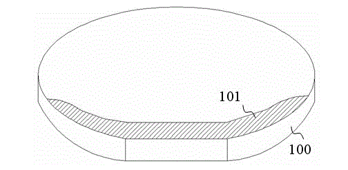
[0030] (1) Refer to figure 1 Prepare a silicon wafer with a thickness of 0.2-0.7 mm, the same diameter and flat side as the ultra-thin product sheet, polished upper surface and ground lower surface as the lining 100, on the upper surface of the flat side and flat sides of the silicon lining 100 Negative photoresist 101 is continuously and evenly coated on the peripheral area of ​​the negative photoresist, the thickness of the negative photoresist is less than 1 millimeter, and the width is within 3 millimeters from the periphery.

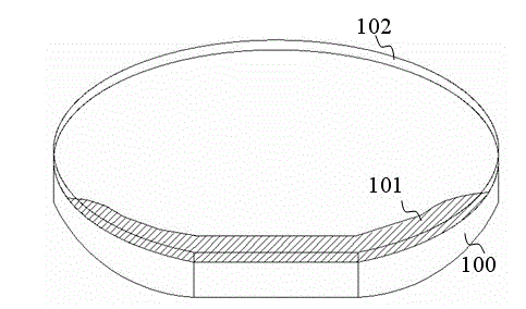
[0031] (2) Refer to figure 2 , put the surface of the ultra-thin silicon product sheet on the upper surface of the silicon lining and stick it on the upper surface of the silicon lining. Keep the flat sid...


PUM


Abstract

The invention discloses a manufacturing method of an ultrathin semiconductor device. The manufacturing method disclosed in the invention comprises the following steps: prepaing a bonding material and a carrier wafer; smearing the bonding material continuously and uniformly on flat surface of the carrier wafer and surrounding areas of upper surface of two sides of the flat surface; pasting one side of ultrathin product sheet to be processed on the upper surface of the carrier wafer and aligning the flat surface; then, processing the other side of the ultrathin product sheet, such as conventional ion implantation, dry etching and the like; after the processing, separating the ultrathin product sheet from the upper surface of the carrier wafer; finally, removing the bonding material on the ultrathin product sheet and the carrier wafer. The method in the invention is simple and stable. Costs are low and the method is easy to be realized. The carrier wafer can be regenerated and used repeatedly. The method is especially suitable for processing a back side of the ultrathin sheet during a manufacturing process of the ultrathin power semiconductor device.

Description

technical field [0001] The invention relates to a manufacturing method of a semiconductor device, in particular to a manufacturing method for an ultra-thin semiconductor device, which is suitable for processing the backside of an ultra-thin power semiconductor device in the manufacturing process. Background technique [0002] In the manufacturing process of semiconductor devices, in order to obtain better mechanical properties, electrical properties, and the needs of subsequent processing technology, it is generally necessary to thin the product sheet, and the thickness after thinning is usually about 200-400 microns. For some special semiconductor devices, especially some power semiconductor devices, in order to obtain thinner chips, or to meet the requirements of better electrical performance, it is necessary to reduce the thickness of the product sheet to be thinner, such as below 200 microns or even up to Below 100 microns, it is processed into a so-called ultra-t...

Claims


Application Information

Patent Timeline
Patent Type & Authority Patents(China)
IPC IPC(8): H01L21/02H01L21/18H01L21/762
Inventor 饶祖刚丛培金沈浩平冯春阳陆界江赵雁高景倩苏雷
Owner TIANJIN HUANXIN TECH DEV
Why Eureka
Try Eureka