Method for measuring transmission of interference-insensitive terahertz wave
A measurement method, terahertz technology, applied in the field of terahertz wave transmission measurement, can solve problems such as output power changes and difficulties, and achieve the effects of eliminating measurement errors, reducing influence, high measurement sensitivity and stability
- Summary
- Abstract
- Description
- Claims
- Application Information
AI Technical Summary
Problems solved by technology
Method used
Image
Examples
Embodiment 1
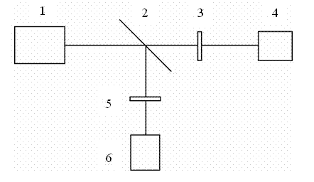
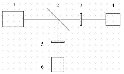
[0031] Measurement of trace amounts of glucose in polyethylene powder. The terahertz wave radiation source is the return wave oscillator OV30 of MicroTech Company. Use a polyethylene lens with a focal length of 50 mm to collimate the divergent terahertz waves radiated by this wave source into parallel propagation. The beam splitter is realized by a piece of high-resistance silicon (13~19KΩ·cm) crystal flat sheet. Each branch uses a 100mm polyethylene lens to focus the terahertz wave onto the sample surface. Terahertz waves transmitted through the sample are focused onto a pyroelectric detector using additional polyethylene lenses. The detection signal is recorded by a lock-in amplifier. The reference signal for the lock-in amplifier is provided by a chopper placed in front of the beam splitter. The chopping frequency of the chopper is 30Hz, and the time constant of the lock-in amplifier is 300ms.
[0032] The terahertz wave with a frequency of 350 GHz was selected to meas...
Embodiment 2
[0034] On-line monitoring of wafer resistance value. Silicon wafer is an important raw material for industries such as integrated circuits and solar cells, and whether its resistivity meets the standard directly affects the performance of the final product. Based on the difference in the absorption of terahertz waves by silicon wafers with different resistivities, an online non-contact non-destructive testing based on terahertz wave transmission measurement is established. The detection device is similar to that in Example 1. A high-resistance silicon wafer with a theoretical thickness of 350 μm was detected using the 315.13 GHz terahertz wave output by the return wave oscillator. Firstly, a 350 μm silicon wafer whose resistivity is exactly the middle value of the specified resistivity is selected as a reference sample. Then measure the absorption of the silicon wafer at the upper and lower critical resistivity points as the judgment standard. Finally, the detection of larg...
PUM
| Property | Measurement | Unit |
|---|---|---|
| Thickness | aaaaa | aaaaa |
Abstract
Description
Claims
Application Information
 - Generate Ideas
- Intellectual Property
- Life Sciences
- Materials
- Tech Scout
- Unparalleled Data Quality
- Higher Quality Content
- 60% Fewer Hallucinations
Browse by: Latest US Patents, China's latest patents, Technical Efficacy Thesaurus, Application Domain, Technology Topic, Popular Technical Reports.
© 2025 PatSnap. All rights reserved.Legal|Privacy policy|Modern Slavery Act Transparency Statement|Sitemap|About US| Contact US: help@patsnap.com


